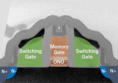
LEE Flash G2 (G2) is an innovative Flash IP offering unique features that no other Flash IP could offer.
It is based on LEE Flash G1, which consists of simple SONOS memory cell, sandwiched by switch transistors on the side.
While maintaining the additional cost at minimum, it requires no high voltage for read operation, no isolation area in-between Memory cells and logic circuits, therefore super low power and easy to layout.
G2’s very special VDD operation architecture enables seamless connection of G2 Flash cell to standard logic circuit. Chip designer now can use non-volatize logic circuit, such as SRAM and open up new possibilities for innovation.
It is cost effective Flash solution for larger memory capacity requirement up to several Mega Bytes.
It also allows user to use standard CMOS process platform as is, utilizing existing PDK and Spice model because the implementation of G2 into the platform does not change any characteristics and geometries of it.
* Due to the ongoing development.
| Item |
Spec |
| Process platform |
55BCD |
| Memory Size |
128K-Byte(1M-bit) |
| P/E Cycles |
100K |
| Supply Voltage |
VDD 1.2V±10% |
| VCC 2.5V~5.5V |
| Additional Masks |
4 |
| Operation Temperature(Tj) |
-10~175℃ |
| Data Retention |
10years@175℃ post PE 10K |
Logic Compatibility
Since no high voltage for program and erase is applied to diffusion layer, all readout circuits are composed of standard core transistors.
It realizes good compatibility with peripheral logic circuits and it becomes possible to mix G2 with logic circuits such as Non Volatile SRAM.
High Speed by VDD operation
Read circuit composed by core transistors realizes high speed access characteristic.
Large Memory Capacity
Read circuit composed by core transistors realizes high speed access characteristic.
Large Programming Size enables Short Testing Time
G2 also uses FN tunneling technology to achieve extremely low power in program and erase.
It consumes 1/1,000,000 times current, compare to conventional technologies using hot carrier injection for program/erase operation.
This also helps reducing testing time, which dominates large portion of the chip cost.
Low cost
Short Test Time: G2 achieves very short test time for two reasons.
- Extremely low power in program/erase allows tester to program/erase the whole memory mat at once, compare to conventional solution program/erase smaller sections for many times to program/erase the whole memory mat.
- Sharp Vt distribution in programming will eliminate the requirement for multiple programming and verification, so that programming operation always completes at one time, not in multiple steps, to dramatically reduce programming time.
Short Baking Time
Floadia’s unique memory architecture simplifies Life Time Prediction of the memory cell, which allows chip company to screen devices with shorter baking time.
4 Mask adder
G2 requires only 4 to 5 additional masks on standard CMOS process, reducing expensive mask cost to implement NVM feature on your chip. Conventional solution will usually take around 10+ additional masks and uses special manufacturing process
Re-use of existing IP asset
Unlike normal Flash IPs, our Flash IP does not affect SPICE model of the logic transistors, which means you can utilize existing IPs and assets that has been developed, and will eliminate additional IP investment specific for Flash ICs