Vendor: T2M GmbH Category: ADC

Dual core I & Q Analog to Digital Converter

This is a dual core I & Q Analog to Digital Converter based on the Time Interleaved SAR architecture.

Overview

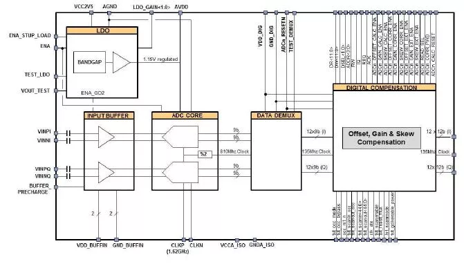
This is a dual core I & Q Analog to Digital Converter based on the Time Interleaved SAR architecture. The IP includes a power supply regulator (LDO), integrated references and digital compensation (for gain, offset and skew). It works in a differential mode for analog input I & Q. The output data are organized in 12x12b–buses clocked at 135MHz (Fs/12). Each bus gives the data coming from a specific sub-ADC. A data ready clock is provided at 135MHz (Fs/12).The input buffers I & Q and the LDO are in G02.The Core ADC and the Digital Compensation are in GO1.

Key features

  • Maturity MAT05
  • 9-bits DUAL-CORE I & Q SAR ADC
  • Up to 1.62Gsps Sampling Rate
  • Analog power supply for Input Buffer: from 1.7V to 2.75V (GO2 domain)
  • Analog power supply for LDO: from 1.7V to 2.75V (GO2 domain)
  • Digital power supply for Data Demux and Digital Compensation: 1.1V (GO1 domain)
  • Input range: 1 Vpp differential for I&Q
  • AC coupling input
  • Input signal bandwidth: 100Hz to 600MHz
  • Power down mode
  • Data ready output at 135MHz
  • Size: Under NDA
  • Power Consumption:
  • Analog: 68mA on GO2 supply
  • Digital Compensation: 36 mA on GO1 supply
  • Technology: under NDA
  • Device types: SVT, LVT, XHPA, GO2 (50Ang; 2.5V), MIM5f Capacitor

Block Diagram

What’s Included?

  • Detailed Specification and Integration guide
  • LEF abstract
  • GDSII layout and Mapping files
  • LVS compatible netlist
  • Verilog-A Model

Specifications

Identity

Part Number
9-Bit Dual Core SAR ADC
Vendor
T2M GmbH
Type
Silicon IP

Provider

HQ: Germany

Learn more about ADC IP core

Uncertainty-Guided Live Measurement Sequencing for Fast SAR ADC Linearity Testing

This paper introduces a novel closed-loop testing methodology for efficient linearity testing of high-resolution Successive Approximation Register (SAR) Analog-to-Digital Converters (ADCs). Existing test strategies, including histogram-based approaches, sine wave testing, and model-driven reconstruction, often rely on dense data acquisition followed by offline post-processing, which increases overall test time and complexity.

Three ways of looking at a sigma-delta ADC device

The growing availability of digital ICs like microcontrollers, microprocessors, and field-programmable gate arrays (FPGAs) allows developers to use complex digital processing techniques rather than analog signal conditioning. For this reason, analog-to-digital converters (ADCs) have become a widely-used component in mixed-signal circuits.

Specifying a PLL Part 1: Calculating PLL Clock Spur Requirements from ADC or DAC SFDR

In high end RF systems, such as 5G radios, the requirements are so stringent that the source of this strongest unwanted tone can be the PLL. This article outlines how spurs in the input clock to the ADC or DAC may limit the SFDR. This in turn will set the requirements for the spurs for the input clock (from a PLL), in order to achieve a specific SFDR.

Save power in IoT SoCs by leveraging ADC characteristics

Power-sensitive applications such as Internet-of-Things (IoT) require a comprehensive power savings strategy within the system-on-chip (SoC). Techniques relying solely on the use of traditional power down modes and low supply voltage may not be enough to achieve the required power targets. The analog block is often assumed to be too sensitive and not compatible with aggressive power management techniques.

High Speed ADC Data Transfer

When continuously running a high speed ADC, it can be a challenge to deal with the firehose of raw data available at the output. To use City Semiconductor’s 2.5 GS/s 12-bit ADC, for example, 30 gigabits per second of data have to be accepted.

Frequently asked questions about ADC IP cores

What is Dual core I & Q Analog to Digital Converter?

Dual core I & Q Analog to Digital Converter is a ADC IP core from T2M GmbH listed on Semi IP Hub.

How should engineers evaluate this ADC?

Engineers should review the overview, key features, supported foundries and nodes, maturity, deliverables, and provider information before shortlisting this ADC IP.

Can this semiconductor IP be compared with similar products?

Yes. Buyers can compare this product with similar semiconductor IP cores or IP families based on category, provider, process options, and structured technical specifications.

×
Semiconductor IP