Vendor:
Digital Blocks, Inc.
Category:
SPI / QSPI XSPI
AMBA Bus Host to eSPI Target
eSPI Target RTL SystemVerilog IP Core
Overview
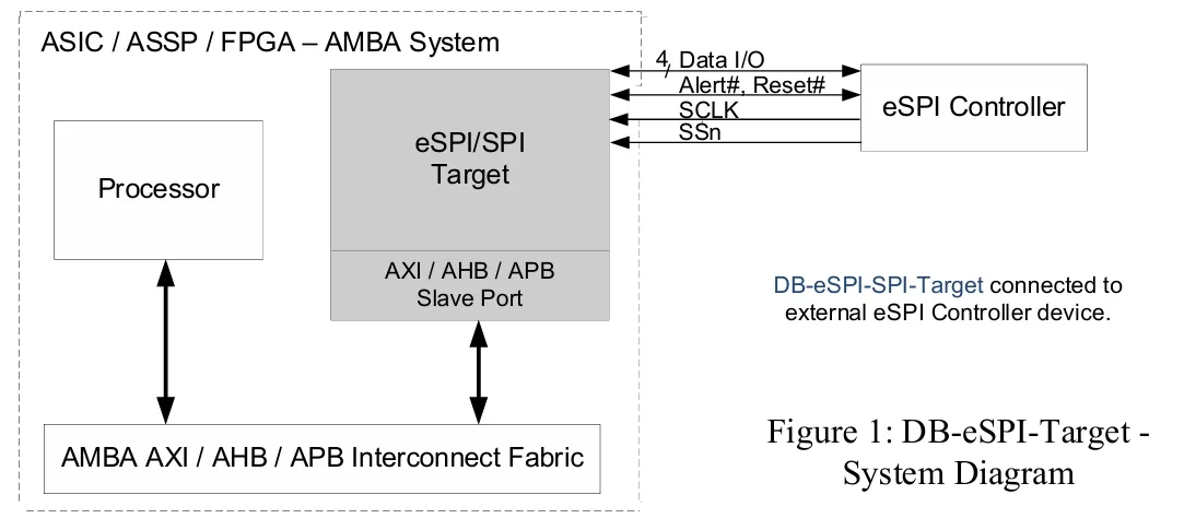
The Digital Blocks DB-eSPI-Target-AMBA is a fully compliant Intel Enhanced Serial Peripheral Interface (eSPI) Base Specification Revision 1.5 (May 2022) eSPI-Target SystemVerilog RTL IP Core, with backward-compatible standard SPI Slave mode for legacy SPI Master hosts. It contains an AMBA AXI, AHB, or APB Bus Interface for connecting a local microprocessor (or memory-mapped subsystem) to an external eSPI Controller.
As an eSPI Target, the DB-eSPI-Target-AMBA responds to PUT_* commands from the Controller (memory writes, virtual-wire updates, OOB messages, flash requests) and supplies completion data, status, and read data on GET_* commands. The IP fully off loads packet framing, CRC-8 generation and checking, per-channel queue-status tracking, and response-code generation from the local microprocessor.
The DB-eSPI-Target-AMBA contains independent dual-clock Transmit and Receive FIFOs and multiple Finite State Machines with comprehensive status and interrupt capability. Optionally, a DMA Controller can transfer data between user memory and the eSPI / SPI Bus.
The DB-eSPI-Target targets ASIC / ASSP / FPGA integrated circuits, where typically the local processor is an Intel, ARM, or RISC-V processor, but any embedded processor is supported. Figure 1 depicts the system view of the DB-eSPI-Target IP Core embedded within a Target SoC, communicating with an external eSPI Controller (and / or legacy SPI Master) on the shared bus.
Separate Digital Blocks DB-eSPI-Controller-AMBA for the Controller side of an eSPI link and combination DB-eSPI-Controller-Target-AMBA releases are available.
Key features
Features – DB-eSPI-Target
The DB-eSPI-Target-AMBA is a fully compliant Intel eSPI Base Specification Rev. 1.5 (May 2022) Target IP core, with backward-compatible standard SPI Slave mode and an AMBA APB / AHB / AXI4-Lite local-side interface.
Standards & Compliance
- Full compliance to eSPI Base Specification Rev. 1.5, Target function (Intel document 327432-005)
- Supports all four eSPI channels — Ch 0 Peripheral, Ch 1 Virtual Wire, Ch 2 Out of-Band Message, Ch 3 Flash Access
- Channel 3 Flash supports both CAFS (Controller-Attached Flash Sharing) and TAFS (Target-Attached Flash Sharing) modes
- Backward-compatible standard SPI Slave mode for legacy SPI Master hosts
Operating Modes & Throughput
- Selectable per-transfer I/O lane width: Single (x1), Dual (x2), or Quad (x4) — accepted from Controller's SET_CONFIGURATION
- Full-duplex eSPI transfers — Command Phase immediately followed by Response Phase on the shared bus
- Programmable channel maximum payload size advertised in GCC / CHxCC capability registers: 64 / 128 / 256 bytes per packet
- Up to 64 Virtual Wire groups supported on Channel 1 (eSPI 1.5 maximum)
- In-Band Reset (IBR) detection on the bus with local interrupt — restores GCC register (Offset 008h-00Bh) to default state per eSPI 1.5 §3.5 eSPI
Sideband Signals
- RESET# — input from the Controller; on assertion, resets all SCK-domain logic and Slave-side configuration (GCC, CHxCC, channel-status). APB-side CSRs (CR1, CR2, ISR, IMR, FIFO thresholds) survive RESET#.
- ALERT# — Target-driven output to the Controller, asserted on local interrupt event
Controller Topology
- Responds to a single bus Controller per eSPI 1.5
Bus & Clocking
- AMBA APB / AHB / AXI4-Lite slave interface for register and FIFO access on the local side
- Independent local APB clock and SCK clock domains; safe CDC via Gray-coded pointer synchronizers throughout
- SCK is received from the external Controller
- Async-assert / sync-deassert reset synchronization on the SCK domain
FIFO Architecture
- Independent dual-clock asynchronous TX and RX FIFOs, default 256 bytes each (parameterizable 4 – 4096 B via *_FIFO_ADDRSIZE)
- Software-readable byte counts and programmable almost-empty / almost-full thresholds per FIFO
- Recommended buffer sizes for Maximum-GCC operation across all four channels documented in the TRM (Section "FIFO Sizing — eSPI Target")
Data Integrity & Protocol Error Handling
- CRC-8 generator on transmit; CRC-8 checker on receive
- Hardware-generated FATAL_ERROR response on: RX CRC mismatch; GET_* with channel TX AVAIL = 0; PUT_NP with NP RX queue FREE = 0; PUT_FLASH_C (CAFS) or PUT_FLASH_NP (TAFS) with Flash RX queue FREE = 0
- Programmable WAIT-STATE response generation
- Hardware-generated DEFER response on WAIT-State timeout
- ACCEPT response with optional channel-specific modifier
Interrupts
- Single combined Interrupt output with per-source mask, status, and vector registers Sources: TX almost-empty, RX almost-full, TX/RX overrun & underrun, slave transfer complete (STC), command / response error, CRC error, In-Band Reset (IBR) detected from Controller
Synthesis & Implementation
- Selectable FIFO memory style — inferred RAM for FPGA Block-RAM / LUTRAM, or register-based for ASIC register-file
- Scan-test ready; clean lint and CDC results
- Validated on Synopsys Design Compiler (ASIC) and FPGA flows (Xilinx Vivado, Intel Quartus)
Features - DB-SPI-Slave (Legacy SPI Mode)
- Standard SPI Slave mode for backward compatibility with legacy SPI Master hosts
- Half-Duplex / Full-Duplex transfers (simultaneous Transmit & Receive in FD mode)
- Four-signal SPI interface: MOSI, MISO, SCK, SS#
- Programmable SPI frame formats
- Programmable LSB-first or MSB-first byte order, per word
- Two clock domains: AMBA Bus clock and SCK clock (SCK driven by external Master)
- Independent dual-clock Transmit / Receive FIFOs — 8-bit data width, configurable depth 4 – 256 bytes, implemented as registers or SRAM
- Optional DMA Controller for memory ↔ SPI Bus transfers
- Internal interrupts with masking control
- Available AMBA / Avalon Microprocessor Interfaces: AXI / AHB / APB / Avalon Buses
- 8-bit / 32-bit Data Interface
- Fully-synchronous, synthesizable SystemVerilog RTL core, with rising-edge clocking, no gated clocks, and no internal tri-states, for easy integration into FPGA or ASIC design flows.
Block Diagram
Click to open fullscreen
What’s Included?
- The DB-eSPI-Target-AMBA is available in synthesizable SystemVerilog RTL or a technology-specific netlist for FPGAs, along with a simulation testbench with expected results, integration guide, C-code bare-metal and Linux driver, and Technical Reference Manual.
Specifications
Identity
Part Number
DB-eSPI-Target-AMBA
Vendor
Digital Blocks, Inc.
Type
Silicon IP
Standards & Interfaces
Protocol_Support
SPI
Files
Note: some files may require an NDA depending on provider policy.
Provider

HQ:
USA
Learn more about SPI / QSPI XSPI IP core
Unleashing the Power of Communication: Exploring the XSPI Protocol and Arasan Chip Systems' XSPI IP Portfolio
Frequently asked questions about SPI / QSPI / xSPI IP cores
What is AMBA Bus Host to eSPI Target?
AMBA Bus Host to eSPI Target is a SPI / QSPI XSPI IP core from Digital Blocks, Inc. listed on Semi IP Hub.
How should engineers evaluate this SPI / QSPI XSPI?
Engineers should review the overview, key features, supported foundries and nodes, maturity, deliverables, and provider information before shortlisting this SPI / QSPI XSPI IP.
Can this semiconductor IP be compared with similar products?
Yes. Buyers can compare this product with similar semiconductor IP cores or IP families based on category, provider, process options, and structured technical specifications.