Vendor: CSEM Category: Edge AI Accelerator

AI/ML Accelerator

Hierarchical scalability is the foundation principle of the Fibonacci machine-learning (ML) system-on-chip (SoC).

Overview

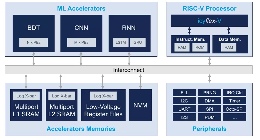
Hierarchical scalability is the foundation principle of the Fibonacci machine-learning (ML) system-on-chip (SoC). Like the Fibonacci number series, combining each element by the sum of the previous ones, the SoC can dynamically increase its computational performance by adding accelerator resources based on the application’s needs. Its heterogenous architecture features a low power time-series ML accelerator (FETA), two clusters of highly parallelized neural processing units (NPU), energy-optimized on-chip memories, a flexible RISC-V microcontroller core, and a rich set of peripherals for easy system integration. Trained models can be deployed through the ML compiler, supporting all common formats (e.g. ONNX).

NPU Clusters

  • Optimized for spatial neural networks (e.g. CNNs, ResNets, MobileNets)
  • Sparsity exploitation
  • Peak MAC performance: 960 GOPS

FETA Cluster

  • Optimized for temporal neural networks (e.g. RNNs like LSTM or GRU)
  • Smart temporal feature extraction engine

Key features

  • General purpose RISC-V core (RV32IMC)
  • Standard communication peripherals: UART, I2C, SPI (x2), Octo-SPI, DCMI, I2S
  • JTAG debugging interface
  • Up to 4 MB of on-chip SRAM + 0.5MB of MRAM
  • Multi neural network execution
  • Selective execution and early exit
  • Dynamic precision scaling
  • Dynamic power switching
  • Bank and block level power gating
  • Flexible DMA engines (x2)
  • Power consumption: 100 uW - 500 mW

Block Diagram

Applications

  • Multi-modal concurrent data analysis from different sensor types (e.g. audio-visual sensor fusion)
  • Multi-stage evaluation: hierarchical execution with increasing complexity to reduce average power consumption.
  • Low power edge processing, down to uW power budgets
  • Spatial and time-series signal analysis

Specifications

Identity

Part Number
Fibonacci
Vendor
CSEM
Type
Silicon IP

Files

Note: some files may require an NDA depending on provider policy.

Provider

HQ: Switzerland

Learn more about Edge AI Accelerator IP core

RISC-V Based TinyML Accelerator for Depthwise Separable Convolutions in Edge AI

While lightweight architectures like MobileNetV2 employ Depthwise Separable Convolutions (DSC) to reduce computational complexity, their multi-stage design introduces a critical performance bottleneck inherent to layer-by-layer execution: the high energy and latency cost of transferring intermediate feature maps to either large on-chip buffers or off-chip DRAM. To address this memory wall, this paper introduces a novel hardware accelerator architecture that utilizes a fused pixel-wise dataflow.

Accelerating Your Development: Simplify SoC I/O with a Single Multi-Protocol SerDes IP

Enter the Multi-Protocol SerDes (Serializer/Deserializer)—a flexible, reusable IP block that allows a single PHY to support multiple serial communication protocols, such as PCIe, SATA, Ethernet, USB, and more. This approach enables SoC vendors to meet diverse customer requirements and application needs without redesigning I/O for each target market.

Frequently asked questions about Edge AI Accelerator IP cores

What is AI/ML Accelerator?

AI/ML Accelerator is a Edge AI Accelerator IP core from CSEM listed on Semi IP Hub.

How should engineers evaluate this Edge AI Accelerator?

Engineers should review the overview, key features, supported foundries and nodes, maturity, deliverables, and provider information before shortlisting this Edge AI Accelerator IP.

Can this semiconductor IP be compared with similar products?

Yes. Buyers can compare this product with similar semiconductor IP cores or IP families based on category, provider, process options, and structured technical specifications.

×
Semiconductor IP