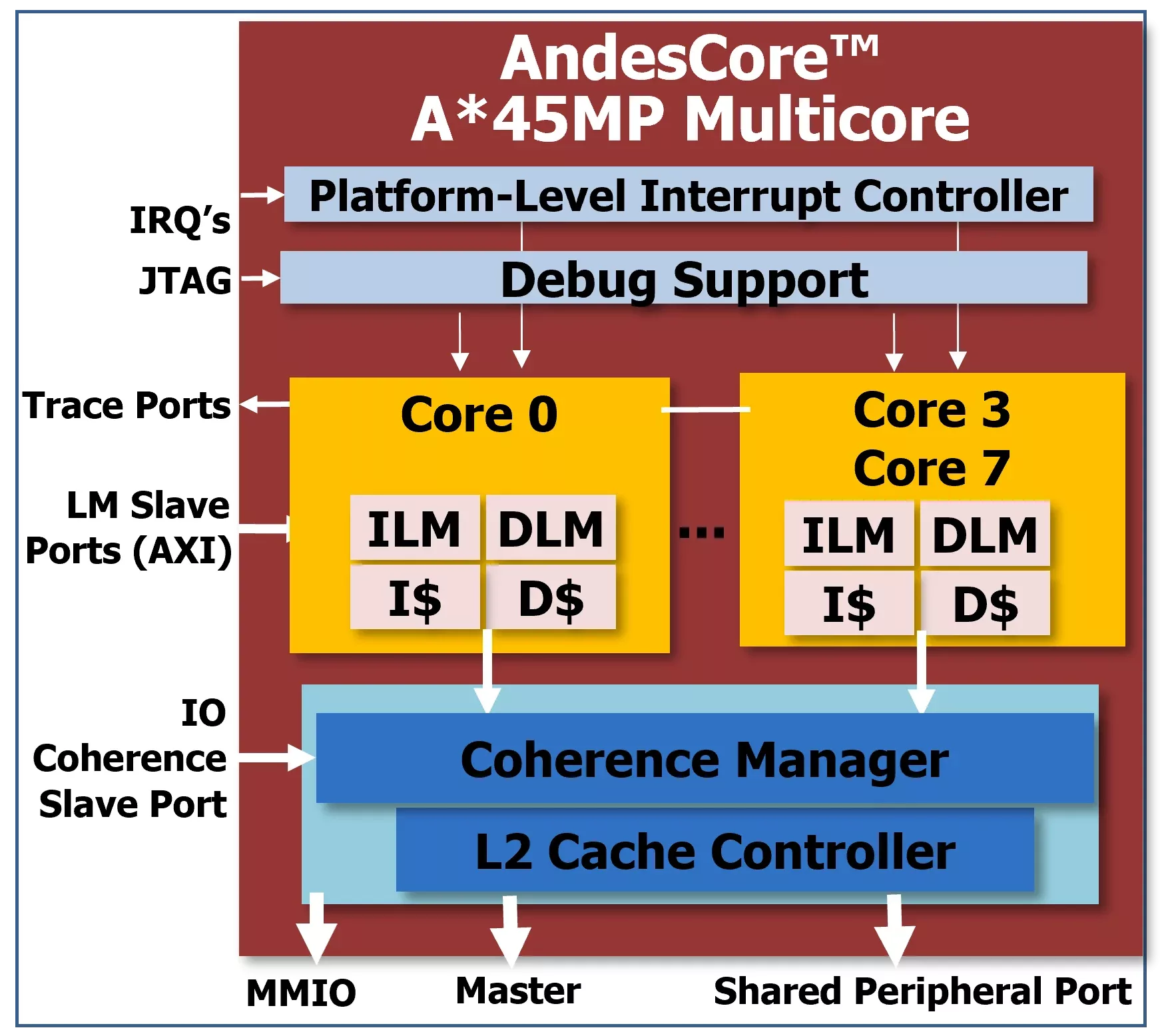
AndesCore™ A45MP 32-bit multicore CPU IP is an 8-stage superscalar processor based on AndeStar™ V5 architecture. It supports RISC-V standard “G (IMA-FD)” extensions, “C” 16-bit compression instructions, DSP/SIMD ‘P’ extension (draft), and Andes performance/ functionality enhancements for faster memory accesses and branch handling, plus Andes Custom Extension™ (ACE) to add user-defined instructions. It features MMU for Linux based applications, branch prediction for efficient branch execution, level-1 instruction/data caches and local memories for low-latency accesses.
The A45MP symmetric multiprocessor supports up to 4 cores and a level-2 cache controller with instruction and data prefetch. It manages level-2 cache coherence including I/O coherence for cacheless bus masters.
Other A45MP features include ECC for level-1/2 memory soft error protection, PLIC with enhancements for vectored dispatch and priority-based preemption, CoDense™ and StackSafe™ for software quality improvement, and suspend to standby/memory, CPU HotPlug, PowerBrake, and WFI for power management.
Key Features and Performance
AndeStar™ V5 Architecture
| Key Features |
Benefits |
| RISC-V RV32GCP instructions |
- State-of-the art ISA from latest developments in computer architecture
- Industry standard and open architecture
|
| Andes Extended Instructions |
Andes exclusive performance and functionality enhancements |
| Andes Custom Extension™ (ACE) option to create custom instructions for software acceleration |
- Add custom instruction extensions to facilitate Domain-Specific Architecture/Acceleration (DSA)
- Boost application performance significantly, at the same time maintain the programmability
- Powerful constructs are available to define high level instruction
- ACE design is based on Verilog and C languages which are familiar to the designers
- The COPILOT tool automatically generates the extended CPU and software toolchain
- Do not require expertise in processor pipeline to design ACE instructions
|
| 16/32-bit mixable instruction format |
For compact code density |
| 32 general-purpose registers |
For better code size and performance |
| Machine (M), User (U) and Supervisor (S) Privilege levels |
For Linux and advanced operating systems with protection between kernel and user programs |
CPU Core
| Key Features |
Benefits |
| 5.67 Coremark/MHz, 2.86 DMIPS/MHz* |
Superior performance-per-MHz |
| 8-stage in-order superscalar pipeline |
Superior performance-efficiency, while allowing for high speeds |
|
Extensive branch predication features
- Branch Target Buffer (BTB)
- Branch Histroy Table (BHT)
- Return Address Stack (RAS)
|
- Branch Target Buffer and Branch History Table to speed up control codes
- Return Address Stack to speeds up procedure returns
|
|
MMU (Memory Management Unit)
- Sv32 virtual-memory systems
- 4/8-entry fully associative ITLB/DTLB
- 32-512-entry 4-way set-associative shared TLB
- Hardware page table walker
|
- Virtual memory support for full address space and easy code/data sharing
- Support for full-featured OS such as Linux
- Protection of supervisor and user privilege
- Hardware for fast address translation
|
| Physical Memory Protection (PMP), configurable up to 32 regions |
Basic read/write/execute memory protection with minimum cost |
| Programmable Physical Memory Attribute (PMA), configurable up to 16 regions |
Configurable memory attributes:
- Memory, I/O, None
- Cacheable/Non-cacheable
- Write-back/Write-through
- Read/write/read & write allocate, no allocate
- Access fault for non-existent regions
|
| Performance monitors |
Program code performance tuning |
| StackSafe™ hardware stack protection |
- Easy identification of stack size threshold during development
- Hardware error detection of stack overflow and underflow at runtime
|
|
Multiplier options
- Fast multiplier: pipelined, 2-cycle
- Small multipliers: producing 1, 2, 4, or 8 bits per cycle
|
Option to choose between speed and area according to application's requirements |
| PowerBrake technology |
Performance throttling to digitally reduce power consumption |
|
Cluster power management
- Suspend to Standby
- Suspend to Memory
- CPU Hotplug
|
Different low power modes for different use cases |
* BSP v5.1.0, DMIPS/MHZ follow Dhrystone’s no-inline ground rules, best performances
Memory Subsystems
| Key Features |
Benefits |
|
Level-1 I-Cache & D-Cache
- Size: 8KB to 64KB
- Cache line size: 64 bytes
- Set associativity: 2-way or 4-way
|
- Accelerating accesses to slow memories
- Flexible cache configurations
|
|
Level-2 I/D Unified Cache
- Configurable from 128KB to 8MB
- 64-byte cache line size
- 16-way, pseudo random replacement
- 2 tag banks, 2 data banks with interleaving
- Configurable memory cycles for SRAM timing
|
- Capture large working-set instruction and data to improve performance
- Flexible selections to meet performance and timing requirements
|
|
ILM & DLM
- Size: 4KB to 16MB
- SRAM interface support
- Bus masters accessed by AXI slave port
|
- For deterministic and efficient program execution
- Flexible size selection to fit diversified needs
|
| MemBoost |
Optimize cache reads and writes to achieve higher bandwidth and lower latency |
| Optional ECC error protection with SRAM interface |
Code and data integrity protection |
| Bus master port: AXI with 128/256-bit data bus |
High throughput with wide data path |
| BUS Slave Port: AXI with 128/256-bit data, for ILM/DLM accesses |
Efficient data transfer between CPU and SoC masters |
| Core/bus clock ratio of N:1 |
Simplified SoC integration |
Multicore Cache Coherence
| Key Features |
Benefits |
- Support up to 4 cores
- MESI cache coherence protocol
- 128/256-bit I/O coherence port for cacheless bus masters
|
- Symmetric multicore and L2 cache controller with cache coherence between level-1 (L1) caches and I/O coherence for bus masters without caches
- Convenient and efficient interface for SoCs with rich I/O transactions
|
Platform-Level Interrupt Controller (PLIC)
| Key Features |
Benefits |
|
Implements RISC-V PLIC specification
- Up to 1023 PLIC interrupt sources
- Up to 255 PLIC interrupt priority levels
- Up to 16 PLIC interrupt targets
|
Allow individual interrupts to be serviced and prioritized without sharing |
|
Enhanced interrupt features
- Vectored interrupt dispatch
- Priority-based preemption
- Selectable edge trigger or level trigger
|
- Faster interrupt handling for real-time applications
- Complete hardware preemption support for faster response
- Flexible interrupt source interface for simpler SoC design
|
Debug Support
| Key Features |
Benefits |
| Implements RISC-V debug specifications ver 0.13 |
Supported by industry debug tool suppliers |
| JTAG Debug Port |
Industry-standard support |
| Embedded Debug Module with up to 8 triggers |
Flexible configurations to tradeoff between gate count and debugging capabilities |
| Exception redirection support |
Entering debugger upon selected exceptions without using breakpoints |
Trace Support
| Key Features |
Benefits |
| Implements RISC-V Trace 1.0 Instruction Trace Interface |
Supported by Andes tools |