Wafer Capacity by Feature Size Shows Strongest Growth at <10nm
Network, cellphone, and graphics processors drive demand for leading edge processes.
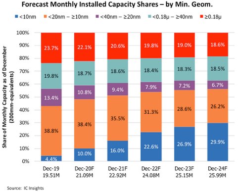
November 17, 2020 -- IC capacity for leading-edge (<10nm) processes is expected to grow and become the largest portion of monthly installed capacity across the industry beginning in 2024, based on information in IC Insights’ Global Wafer Capacity 2020-2024 report. At the end of 2020, <10nm capacity is expected to account for 10% of the IC industry’s total wafer capacity, and then is forecast to rise above 20% for the first time in 2022, and increase to 30% of worldwide capacity in 2024 (Figure 1). What constitutes a generation and how to measure the minimum process geometry gets more difficult every year. Therefore, any assumptions made regarding the wafer fab capacity of new process technologies can have a big impact on the forecast for wafer capacity by minimum feature size.

Figure 1
There is tremendous motivation to continue shrinking minimum geometries because the benefits are many: higher speed, lower power consumption, lower cost per unit area, etc., but there comes a point where diminishing returns make chip designers question whether the high cost is worth it. The cost benefits of scaling aren’t what they used to be.
Equipment costs associated with <10nm process technologies have soared to the point where they have become prohibitive for many IC suppliers. Consequently, only Samsung, TSMC, and Intel currently operate fabs using <10nm process technology.
Meanwhile, design difficulties (for example, continuing to shrink DRAM and NAND flash memory cells) stand in the way of the scaling methods that the IC industry has used for many years. Challenges are also mounting for complex logic-based chips such as microprocessors, ASICs, FPGAs, and other advanced logic devices.
IC Insights believes the pace of migration of finer feature sizes for complex logic-based chips will continue slowing as chip designers find it increasingly difficult to justify the higher costs. For applications that greatly benefit from higher speeds, lower power consumption, etc, there will be healthy demand for the leading-edge finFET processes and beyond. The roll out of half-step generations or enhanced versions of existing processes is also contributing to more time passing between each new generation node.
Other findings from the Global Wafer Capacity 2020-2024 report include,
- In 2020 48% of all wafer capacity is expected to be for devices having minimum geometries (or equivalent minimum geometries) smaller than 20nm (10.0% at <10nm; 38.4% at 10-20nm). Such devices include high-density DRAM and high-density 3D NAND flash with equivalent 10nm-class technology, high-performance microprocessors, low-power application processors, and advanced ASIC/ASSP/FPGA devices based on 16/14nm, 12/10nm, or 7/5nm technologies.
- South Korea, with 66% of its capacity dedicated to <20nm process technology, remains significantly more leading-edge focused than the other regions or countries. Given Samsung and SK Hynix’s emphasis on high-density DRAM, flash memory, and Samsung’s applications processors, it is not a surprise that the country has the highest concentration of wafer capacity dedicated to leading-edge processes.
- Apple, Huawei, and Qualcomm use TSMC’s leading-edge logic foundry services. As a result, Taiwan’s total <20nm capacity stands at more than 35%. Nevertheless, the 28nm, 45/40nm, and 65nm generations continue to generate significant business volumes for foundries like TSMC and UMC.
- Most <20nm capacity in China is owned and controlled by foreign companies, namely Samsung, SK Hynix, Intel, and TSMC. YMTC and SMIC are the only China-based companies that offer <20nm process technology.
Report Details: Global Wafer Capacity 2020-2024
IC Insights’ Global Wafer Capacity 2020-2024—Detailed Analysis and Forecast of the IC Industry’s Wafer Fab Capacity report assesses the IC industry’s capacity by wafer size, minimum process geometry, technology type, geographic region, and device type through 2024. The report includes detailed profiles of the companies with the greatest fab capacity and gives comprehensive specifications on existing wafer fab facilities. Global Wafer Capacity 2020-2024 is priced at $4,890 for an individual user license. A multi-user worldwide corporate license is available for $7,590.
Related Semiconductor IP
- UCIe D2D Adapter & PHY Integrated IP
- Low Dropout (LDO) Regulator
- 16-Bit xSPI PSRAM PHY
- MIPI CSI-2 CSE2 Security Module
- ASIL B Compliant MIPI CSI-2 CSE2 Security Module
Related News
- Samsung, TSMC Remain Tops in Available Wafer Fab Capacity
- Taiwan Passes South Korea to Become #1 in Total IC Wafer Fab Capacity
- Companies Maximizing 300mm, 200mm Wafer Capacity
- Taiwan Maintains Largest Share of Global IC Wafer Fab Capacity
Latest News
- GUC Announces 3nm 12 Gbps HBM4 PHY and Controller
- Arasan acheives the Industry's First ASIL-D Certification for its CAN XL IP Core
- Quintauris and Elektrobit Partner to Enable Reliable RISC-V Solutions for Automotive
- Wind River Joins the CHERI Alliance and Collaborates with Innovate UK to Accelerate Cybersecurity Innovation
- Arteris and MIPS Partner to Accelerate Development for Physical AI Platforms