Samsung's Big Semi Capex Spending Keeps Pressure on Competition
Samsung’s two-year capex spending of $46.8 billion nearly matches the combined two-year capex spending of $48.4 set by Intel and TSMC.
November 30, 2018 -- IC Insights revised its outlook for total semiconductor industry capital spending and presented its forecast of semiconductor capex spending for individual companies in its November Update to The McClean Report 2018, which was released earlier this month.
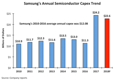
Samsung is expected to have the largest capex budget of any IC supplier again in 2018. After spending $24.2 billion for semiconductor capex in 2017, IC Insights forecasts that Samsung’s spending will edge slightly downward, but remain at a very strong level of $22.6 billion in 2018 (Figure 1). If it comes in at this amount, Samsung’s two-year semiconductor capital spending will be an astounding $46.8 billion.

Figure 1
As seen in Figure 1, Samsung’s semiconductor capital outlays from 2010, the first year the company spent more than $10 billion in semiconductor capex, through 2016 averaged $12.0 billion per year. However, after spending $11.3 billion in 2016, the company more than doubled its 2017 capex budget. The fact that Samsung’s continued its strong capex spending in 2018 is just as impressive.
IC Insights believes that Samsung’s massive spending outlays in 2017 and 2018 will have repercussions far into the future. One effect that has already begun is a period of overcapacity in the 3D NAND flash market. This overcapacity situation is due not only to Samsung’s huge spending for 3D NAND flash, but also from spending by competitors (e.g., SK Hynix, Micron, Toshiba, Intel, etc.) that attempt to keep pace in this market segment.
With the DRAM and NAND flash memory markets showing strong growth through the first three quarters of 2018, SK Hynix ramped up its capital spending this year. In 1Q18, SK Hynix said that it intended to increase its capex spending by “at least 30%” this year. In the November Update, IC Insights forecasts that SK Hynix will see a 58% surge in its semi capex spending. The increased spending by SK Hynix this year is focused primarily on bringing new capacity online at two of its large memory fabs—M15, a 3D NAND flash fab in Cheongju, South Korea, and the expansion of its huge DRAM fab in Wuxi, China. The Cheongju fab is being pushed to open before the end of this year. The Wuxi fab is also targeted to open by the end of this year, a few months earlier than its original start date of early 2019.
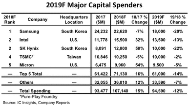
Overall, IC Insights’ now forecasts total semiconductor industry capital spending will climb 15% to $107.1 billion this year, the first time that annual industry capex is expected to top $100.0 billion. Following the industry-wide growth this year, semiconductor capex is expected to decline 12% in 2019 (Figure 2).

Figure 2
Given that the current softness in the memory market is expected to extend into at least the first half of next year, the combined capital spending by the three largest memory suppliers—Samsung, SK Hynix, and Micron—is forecast to drop from $45.4 billion in 2018 to $37.5 billion in 2019, a decline of 17%.
In total, the top five spenders, which are expected to represent 66% of total outlays this year, are forecast to cut their capital spending by 14% in 2019 with the remaining semiconductor industry companies registering a 7% decline.
Report Details: The McClean Report 2019
The 2019 edition of The McClean Report—A Complete Analysis and Forecast of the Integrated Circuit Industry, will be released in January 2019. A subscription to The McClean Report includes free monthly updates from March through November (including a 200+ page Mid-Year Update), and free access to subscriber-only webinars throughout the year. An individual user license to the 2019 edition of The McClean Report is priced at $4,990 and includes an Internet access password. A multi-user worldwide corporate license is available for $7,990.
As part of your 2019 subscription, you are entitled to free attendance at a McClean Report seminar (one seat for each copy purchased; company-wide licensees receive five free seats). The schedule for next year’s seminar tour is shown below.
- Tuesday, January 22, 2019 — Scottsdale, Arizona
- Thursday, January 24, 2019 — Sunnyvale, California
- Tuesday, January 29, 2019 — Boston, Massachusetts
Related Semiconductor IP
- UCIe D2D Adapter & PHY Integrated IP
- Low Dropout (LDO) Regulator
- 16-Bit xSPI PSRAM PHY
- MIPI CSI-2 CSE2 Security Module
- ASIL B Compliant MIPI CSI-2 CSE2 Security Module
Related News
- Asia-Pac Soars, Japan Drops in Regional Semiconductor Capex Spending
- Samsung Still Spending Heavily on Capex
- Flash Memory Remains Primary Target for Capex Spending
- DRAM Capex Spending Expected to Decline 20% in 2020
Latest News
- Wind River Joins the CHERI Alliance and Collaborates with Innovate UK to Accelerate Cybersecurity Innovation
- Arteris and MIPS Partner to Accelerate Development for Physical AI Platforms
- DCD-SEMI expands CryptOne with EdDSA Curve25519 IP core for secure embedded systems
- Syntacore's SCR RISC-V IP Now Supports Zephyr 4.3
- Xylon Presents New 12-Channel GMSL3/GMSL2 FMC+ ExpansionBoard