Flash Memory Remains Primary Target for Capex Spending
2019 to be third year of greater than $25.0B in spending for flash, topping both DRAM, foundry.
January 11, 2019 -- IC Insights is in the process of completing its forecast and analysis of the IC industry and will present its new findings in The McClean Report 2019, which will be published later this month. Among the semiconductor industry data included in the new 400+ page report is an in-depth analysis of semiconductor capex spending.
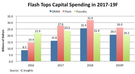
The semiconductor industry is expected to allocate the largest portion of its capex spending for flash memory again in 2019, marking the third consecutive year that flash has led all other segments in spending (Figure 1). Flash memory trailed the foundry segment in capex in 2016, but took an extra-large jump in 2017, growing 92% to $27.6 billion and increased another 16% to $31.9 billion in 2018 as manufacturers expanded and upgraded their production lines for 3D NAND to meet growing demand. With much of the expansion now completed or expected to be wrapped up in 2019, flash capex is forecast to decline 18% this year to $26.0 billion, which still is a very healthy spending level.

Figure 1
- In 2018, SK Hynix completed and opened M15 its new wafer fab facility in Cheongju, South Korea. First devices produced from the factory were 72-layer 3D NAND flash.
- Micron allocated significant resources to upgrade its two existing flash fabs in Singapore and broke ground on construction of a third NAND wafer fab there.
- Toshiba Memory completed construction of a new 300mm wafer plant (Fab 6) at its Yokkaichi site in 1H18. Operations at Phase 1 of the facility are expected to begin in early 2019. Also, Toshiba announced that its next flash memory fab after Fab 6 would be located in Kitakami, Iwate. The company broke ground on this fab in July 2018.
- XMC/Yangtze River Storage Technology (YMTC), which is owned by Tsinghua Unigroup, completed construction of its new fab, installed equipment, and began small-volume production of 32-layer 3D NAND flash.
- Samsung and all of the other “legacy” flash suppliers are well aware of the big plans that China has to be a player in the 3D NAND flash market. Samsung will continue to invest heavily to stay far ahead of existing competitors or new startups and maintain its competitive edge against any who think they can wrestle marketshare away. Samsung spent $13.0 billion on flash capex in 2017 and $9.0 billion in 2018, accounting for 28% of the total $31.9 billion in flash memory capital spending last year. IC Insights estimates Samsung will spend another $7.0 billion for flash capex in 2019.
Report Details: The 2019 McClean Report
Details and forecasts of industry-wide capital spending, including a 2018 ranking of top capital spenders, are included in the 2019 edition of The McClean Report—A Complete Analysis and Forecast of the Integrated Circuit Industry, which will be released in late January 2019. A subscription to The McClean Report includes free monthly updates from March through November (including a 200+ page Mid-Year Update), and free access to subscriber-only webinars throughout the year. An individual user license to the 2019 edition of The McClean Report is priced at $4,990 and includes an Internet access password. A multi-user worldwide corporate license is available for $7,990.
As part of your 2019 subscription, you are entitled to free attendance at a McClean Report half-day seminar (one seat for each copy purchased; company-wide licensees receive five free seats). The schedule for this year’s McClean Report seminar tour is shown below.
Tuesday, January 22, 2019 — Scottsdale, Arizona
Thursday, January 24, 2019 — Sunnyvale, California
Tuesday, January 29, 2019 — Boston, Massachusetts
Related Semiconductor IP
- UCIe D2D Adapter & PHY Integrated IP
- Low Dropout (LDO) Regulator
- 16-Bit xSPI PSRAM PHY
- MIPI CSI-2 CSE2 Security Module
- ASIL B Compliant MIPI CSI-2 CSE2 Security Module
Related News
- Asia-Pac Soars, Japan Drops in Regional Semiconductor Capex Spending
- Mobiveil to Target Its Universal NOR Flash Controller (U-NFC) to Support Adesto Technologies New eXecute-in-Place Non-volatile Memory (NVM) EcoXiP Chip
- Most of 2017 Capital Spending Will Go to Foundry and Flash Memory
- Samsung Still Spending Heavily on Capex
Latest News
- Wind River Joins the CHERI Alliance and Collaborates with Innovate UK to Accelerate Cybersecurity Innovation
- Arteris and MIPS Partner to Accelerate Development for Physical AI Platforms
- DCD-SEMI expands CryptOne with EdDSA Curve25519 IP core for secure embedded systems
- Syntacore's SCR RISC-V IP Now Supports Zephyr 4.3
- Xylon Presents New 12-Channel GMSL3/GMSL2 FMC+ ExpansionBoard