Unveiling the Availability of Industry's First Silicon-Proven 3nm, 24Gbps UCIe™ IP Subsystem with TSMC CoWoS® Technology
Multi-protocol subsystem delivers 8 Tbps/mm bandwidth density and 24 Gbps D2D data rate for hyperscale, HPC, and AI applications
LONDON, United Kingdom, and TORONTO, Canada – September 30, 2024 – Alphawave Semi (LSE: AWE), a global leader in high-speed connectivity and compute silicon for the world’s technology infrastructure, has unveiled the availability of the industry’s first 3nm silicon-proven Universal Chiplet Interconnect Express (UCIe™) Die-to-Die (D2D) IP subsystem, built on TSMC’s Chip-on-Wafer-on-Substrate (CoWoS®) advanced packaging technology.
This complete PHY and controller subsystem, developed in close collaboration with TSMC, is tailored for high-demand applications such as hyperscale data centers, high-performance computing (HPC), and AI. Utilizing TSMC’s CoWoS 2.5D silicon-interposer-based packaging, the fully integrated and highly configurable subsystem delivers a high bandwidth density of 8 Tbps/mm while optimizing I/O complexity, power efficiency, and latency.
The subsystem supports multiple industry protocols—including PCIe®, CXL™, AXI-4, AXI-S, CXS, and CHI—ensuring interoperability across the growing chiplet ecosystem. Additionally, it features live per-lane health monitoring to boost system robustness and operates at speeds of 24 Gbps to meet the bandwidth needs of advanced D2D connectivity.
This UCIe IP subsystem is now available following extensive characterization of the silicon received from TSMC. Alphawave Semi’s team has rigorously validated it against UCIe standards and specifications, across various process conditions (typical, slow, and fast), and under the targeted voltage and temperature conditions.
The successful validation of D2D link margin, TXIO, and RXIO loopback margins reinforces the readiness of Alphawave Semi’s UCIe IP subsystem for integration into customer SoC designs, supporting next-generation HPC and AI applications.

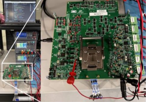
Figure: Alphawave Silicon Validation Setup for UCIe IP Subsystem.
“Achieving successful silicon validation of 3nm 24 Gbps UCIe subsystem with TSMC’s advanced packaging is a significant milestone for Alphawave Semi and underscores the company’s expertise in utilizing the TSMC 3DFabric™ ecosystem to deliver top-tier connectivity solutions,” said Mohit Gupta, Alphawave Semi’s SVP and GM, Custom Silicon and IP.
Gupta also stated the IP sets “a new benchmark in high-performance connectivity solutions.”
“Our recent collaboration with Alphawave Semi exemplifies how we collaborate with our Open Innovation Platform® (OIP) ecosystem partners to enable significant advancements in packaging, meeting the increasing demands in AI and HPC applications,”said Dan Kochpatcharin, Head of Ecosystem and Alliance Management Division at TSMC. “We will continue our partnership with Alphawave Semi to advance the 3D IC design ecosystem to empower faster and power-efficient semiconductor designs.”
Alphawave Semi’s UCIe IP subsystem complies with the latest UCIe Specification Rev 2.0 and includes comprehensive testability and debug features such as JTAG, BIST, DFT, and Known Good Die (KGD) capabilities.
The availability of this 3nm 24Gbps UCIe IP subsystem with TSMC CoWoS® Packaging follows Alphawave Semi’s February 2024 announcement stating its 3nm UCIe IP subsystem with standard packaging was silicon proven (link) and June’s release on the industry’s first multi-protocol chiplet (link).
For more information on Alphawave Semi’s UCIe IP, please visit https://awavesemi.com/silicon-ip/phy-ip/die-to-die-phy-ip/.
For more information on Alphawave Semi, please visit http://awavesemi.com.
To learn more about Alphawave Semi’s latest technology announcements, please visit https://awavesemi.com/company/press-releases/.
About Alphawave Semi
Alphawave Semi is a global leader in high-speed connectivity and compute silicon for the world's technology infrastructure. Faced with the exponential growth of data, Alphawave Semi's technology services a critical need: enabling data to travel faster, more reliably, and with higher performance at lower power. We are a vertically integrated semiconductor company, and our IP, custom silicon, and connectivity products are deployed by global tier-one customers in data centers, compute, networking, AI, 5G, autonomous vehicles, and storage. Founded in 2017 by an expert technical team with a proven track record in licensing semiconductor IP, our mission is to accelerate the critical data infrastructure at the heart of our digital world. To find out more about Alphawave Semi, visit: awavesemi.com.
Related Semiconductor IP
- UCIe D2D Adapter & PHY Integrated IP
- UCIe RX Interface
- AXI-S Protocol Layer for UCIe
- UCIe PHY (Die-to-Die) IP
- UCIe Controller baseline for Streaming Protocols for ASIL B Compliant, AEC-Q100 Grade 2
Related News
- Alphawave Semi Taped-Out Industry Leading 64Gbps UCIe™ IP on TSMC 3nm for the IP Ecosystem, Unleashing Next Generation of AI Chiplet Connectivity
- Alphawave Semi Spearheads Chiplet-Based Custom Silicon for Generative AI and Data Center Workloads with Successful 3nm Tapeouts of HBM3 and UCIe IP
- Alphawave Semi Demonstrates 3nm Silicon-Proven 24Gbps Universal Chiplet Express (UCIe) Subsystem for High-Performance AI Infrastructure
- Alphawave Semi Launches Industry's First 3nm UCIe IP with TSMC CoWoS Packaging
Latest News
- EU DARE Project Is Scrambling to Replace Codasip
- Sofics and Alcyon Photonics Partner to Support Next-Generation Photonic Systems
- QuickLogic Appoints Quantum Leap Solutions as Authorized Sales Representative
- Cadence and NVIDIA Expand Partnership to Reinvent Engineering for the Age of AI and Accelerated Computing
- Cadence and Google Collaborate to Scale AI-Driven Chip Design with ChipStack AI Super Agent on Google Cloud