Overview
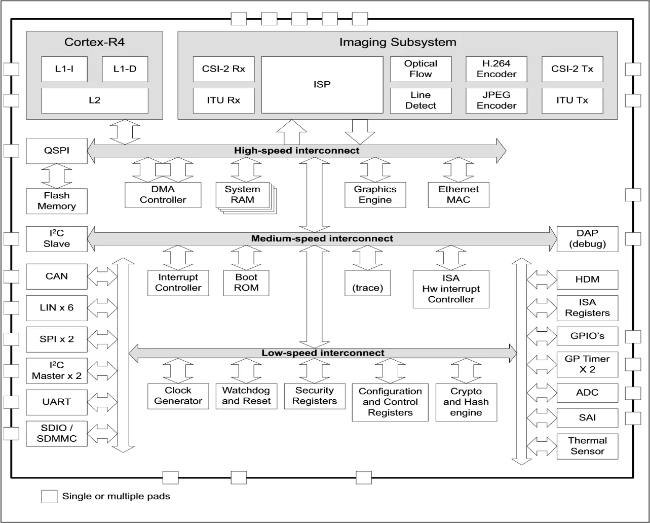
This is a versatile system-on-chip device designed for automotive, security and a multitude of other camera applications. From video and audio input through HDR image signal processing, lens distortion correction, graphics overlay, video compression, video analytics acceleration, CPU, operating and non-volatile memory, media access controller, to video and audio outputs and communication interfaces, it comprises all elements to support compact, low bill-of-material and low energy-consumption camera applications. No external memory chips such as DRAM or Flash are required for its operation, predictive H.264 video encoding inclusive. Resulting ready-for-display video can be output as-is over the parallel or serial video output port, or real-time compressed for streaming out through one of: RGMII/GMII, SDIO or SPI interfaces. An audio signal can be input through either an I2S or a PDM input, processed by the CPU and inserted into the output data stream. A return audio channel is also supported, outputting the audio on an I2S output. Precise Time Protocol (PTP) support and other provisions on the die allow precise instant-of-exposure synchronization of cameras in a multi-camera system, independent of cable lengths. A cryptographic and hash unit permits protection of customer intellectual property embedded in their software. Flash content can be updated via communication interfaces, thus allowing non-intrusive customer firmware updates. A debug access port (DAP) helps users in their software
Learn more about ISP Image Signal Processor IP core
T2M-IP, the global leader in semiconductor IP cores and technology expertise, is proud to announce the immediate availability of its partner's VESA-compliant DisplayPort v1.4 Rx PHY and Controller IP Cores.
T2M announces the availability of its partner’s Bluetooth V6.0 RF Transceiver IP Core in 22nm ULL and 40nm ULP.
Incorporating BroadR-Reach™ technology for Automotive Excellence, this PHY delivers exceptional performance for automotive and industrial applications, providing a superior alternative to traditional BaseT1 solutions.
Designed to meet the evolving needs of next-generation automotive and industrial applications, the CAN XL Controller IP offers superior performance and flexibility while maintaining backward compatibility with previous CAN standards.
T2MIP, a leading provider of semiconductor IP cores, proudly announces the immediate availability of their partner's H.264 and H.265 HEVC Codec IP cores.
T2M-IP is excited to announce that its state-of-the-art USB 3.0 IP, developed in the 22nm ULP (Ultra Low Power) and ULL (Ultra Low Leakage) process technologies, has been successfully licensed to over 10 customers worldwide in the past two years.