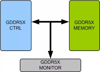
Overview
GDDR5X Memory Model provides an smart way to verify the GDDR5X component of a SOC or a ASIC. The SmartDV's GDDR5X memory model is fully compliant with standard GDDR5X Specification and provides the following features. Better than Denali Memory Models.
GDDR5X Memory Model is supported natively in SystemVerilog, VMM, RVM, AVM, OVM, UVM, Verilog, SystemC, VERA, Specman E and non-standard verification env
GDDR5X Memory Model comes with optional Smart Visual Protocol Debugger (Smart ViPDebug), which is GUI based debugger to speed up debugging.
Learn more about GDDR IP core
This paper will include a short review of the key features of DDR, GDDR and MobileDDR memory architectures, covering power, speed and cost characteristics as well as key functionality differences that can impact overall system architecture. Using real system design experiences each of the main memory architectures will be used to address system design challenges of sustained bandwidth, reliability, access priority, power savings, and interface requirements.
Large Language Models (LLMs) have gained popularity in recent years, driving up the demand for inference. LLM inference is composed of two phases with distinct characteristics: a compute-bound prefill phase followed by a memory-bound decode phase. This paper proposes SPAD (Specialized Prefill and Decode hardware), adopting a less-is-more methodology to design specialized chips tailored to the distinct characteristics of prefill and decode phases.
HBM4 is the latest generation of the High Bandwidth Memory (HBM) that has become analogous to the Artificial Intelligence (AI) boom that is everywhere in today’s world. HBM is also increasingly being used in other applications like Data centers, autonomous driving systems, servers, cloud computing just to mention few domains where bandwidth and performance in a key requirement.
The rapid evolution of artificial intelligence (AI) is reshaping the technological landscape, driving unprecedented demands on computing infrastructure. At the heart of this transformation lie innovations in intellectual property (IP) that enable scalable, efficient, and performance-driven AI factories.
This white paper will discuss the design challenges that IC designers are facing when developing the new GDDR 7 high-performance memory interface and highlight some of the possible solutions to overcome these challenges, ensuring compliance and robustness of the GDDR7 memory interface.
The rapid evolution of artificial intelligence (AI) over the past decade has reshaped the way we interact with technology and transformed industries across the board. From early predictive models and voice assistants to today’s highly complex generative AI systems, we are witnessing the dawn of a new era: AI 2.0.