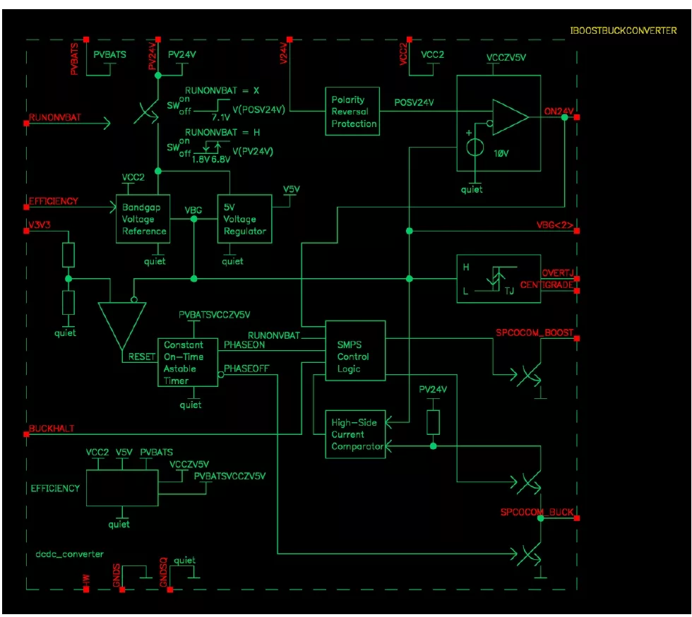
The TS_SPLITPI_3V3_X8 is a variable-frequency switching-mode power converter that regulates voltage on terminals V3V3 and VCC2 to typically 3.3V, either from 10V or more on sense-input V24V and power-input PV24V in buck-mode or from battery voltage as low as 1.9V in boost-buck mode, with the addition of discrete inductors, capacitors and diodes.
Mode switchover is controlled by voltage detection on V24V. For a voltage greater than 10V, buck-only mode operation is signalized by ON24V assertion. The minimum bill of material requires the buck inductor, the smoothing capacitor and optionally a polarity-reversal protecting diode between terminals V24V (anode) and PV24V (cathode). V24V is internally protected against voltage polarity reversal before detection.
For circuit applications running on a battery, the bill of material additionally requires the boost inductor, the flyback diode and a smoothing capacitor to terminal PV24V, to achieve a split-pi topology. Boost-buck mode regulation starts for battery voltage on terminal PVBATS greater than 1.9V.
Voltage regulation precision within ±0.1V is achievable for load current intensities up to 200mA in buck-only-mode and up to 133mA in batterysupplied boost-buck-mode.
Power cycling of V3V3 and VCC2 is possible by asserting input BUCKHALT.
Input RUNONVBAT set low turns off the converter, which then draws from a 2.2V battery less than 2.2nA max on PVBATS and 6nA max on PV24V.
The high-side switch between terminals PV24V and SPCOCOM_BUCK is protected against current intensity rising beyond typically 800mA.
Typical power buck conversion efficiency in case of 10V on V24V amounts to 89% at 200mA load, 82% at 25mA and 64% at 12.1mA.
The TS_SPLITPI_3V3_X8 provides its low-pass filtered bandgap reference voltage on pin VBG<2>, typically 1.247V at 27°C junction temperature with a variation of -1.2mV to 150°C.
The TS_SPLITPI_3V3_X8 contains TES junction overtemperature detector IP, TS_TEMP_DET_X8, providing outputs OVERTJ and CENTIGRADE.
The minimum continuous operation lifetime spans 100000 hours.
Technology: X-FAB XT018-0.18μm BCD-on-SOI CMOS
OPERATING CONDITIONS
| Parameters |
Values / Type |
| Junction temperature range |
-40ºC up to +150ºC |
| Supply voltages with respect to ground GNDS and GNDSQ |
PVBATS: 1.9V up to 3.6V
V24V, PV24V: 10V up to 30V |
| Maximum DC load current intensity |
Buck-only mode: 200mA
Boost-buck mode: 133mA |
| ON24V, VBG<2>, OVERTJ and CENTIGRADE output loads |
CMOS respectively PMOS gate |
SPECIFICATION
| Parameters |
Values / Type |
| Reference voltage at 27°C junction temperature |
VBG: 1.247V (±8.5mV) |
| Reference voltage maximum deviation up to 150°C |
ΔVBG: -1.2mV (±3.5mV) |
| V3V3, VCC2 regulated voltage |
3.3V (±0.1V) |
| Switching frequency upon V3V3, VCC2 voltage rising |
2MHz (±0.5MHz) |
| High-side switch on-time without overcurrent-triggered interrupt |
420ns (±100ns) |
| High-side switch current limiter threshold |
800mA (±300mA) |
| 2.2V-battery-supplied shutdown current consumption (RUNONVBAT = L, V24V terminal unconnected or grounded) |
PVBATS: 0.46nA (max 2.2nA, min 0.42nA)
PV24V: 0.1nA (max 6nA, min 0.06nA)
SPCOCOM_BOOST: 28pA (4.1nA, min 7pA) |
| OVERTJ logic-H voltage |
VCC2 voltage |
| Detector low-going temperature threshold (OVERTJ toggles to logic-L as junction temperature falls) |
138.2°C ± 5.3°C (± 3 sigma) |
| Detector hysteresis (high-going low-going temperature threshold difference) |
9°C ± 1.5°C (± 3 sigma) |
| CENTIGRADE output voltage at 10°C junction temperature |
99.5mV typical |
| CENTIGRADE output voltage slope up to 150°C |
+8.99mV/°C typical |
| Operating power consumption |
252mW max at V(V24V) = 30V, ILOAD = 200mA |
| Area |
1.04mm² |