Overview
The AI and HPC industries are advancing toward chiplet-based designs to achieve superior performance, as traditional monolithic SoCs face scaling challenges. Heterogeneous integration is driving semiconductor innovation but adds complexity to chip design, requiring advanced testing methodologies and improved Automated Test Equipment (ATE). Increasing test patterns and limited package pins demand high-bandwidth IOs, while advancements in ATE capabilities further necessitate optimized GPIOs to support higher-speed, efficient and low-cost testing.
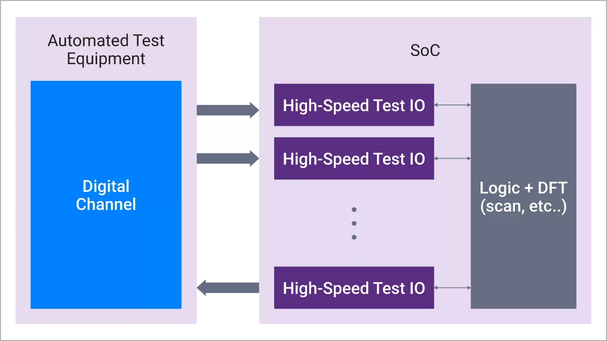
Synopsys High-Speed Test IO IP is a cutting-edge IO interface solution that enables efficient, high-speed testing of complex semiconductor designs while minimizing hardware complexity and cost. It achieves this by supporting high data rates (up to 2.5Gbps) for testing, reusing limited package pins for multiple modes (serving as test ports during manufacturing, enabling high-speed clock observation during debugging, and functioning as GPIO during production), and eliminating the need for complex protocols or calibration sequences. This simplifies testing, reduces development time and costs, and ensures high test coverage and reliability for advanced AI, HPC, and chiplet-based designs.
Learn more about High-Speed IP core
This post provides an in-depth look at the fundamentals of high-speed interconnects, AI/HPC trends (HBM/D2D/CPO), and the three critical requirements of Physical AI: Deterministic Latency, Functional Safety (ISO 26262), and Automotive Reliability (AEC-Q100).
Innosilicon, a leading IP provider, offers a complete PCIe 5.0 solution stack that includes both PHY and controller IPs. Although both layers are crucial to achieving a fully compliant and high-performance PCIe interface, this paper deep dives into the technical challenges of PHY design, highlighting insights drawn from real-world design margins, receiver robustness, and advanced jitter analysis in the context of Gen5 systems.
LTTPR support is quickly becoming a cornerstone of next-gen DisplayPort architectures, particularly in automotive, industrial, and multi-display environments. Here's what you need to know.
Protocol standards and speeds are advancing rapidly to boost productivity and efficiency for high-performance computing (HPC), AI training, and other applications, with the arrival of PCI Express (PCIe) 7.0 being the latest example.
Maximize limited package pins with IO that can act as high-speed test ports then be reused as low-power GPIOs during field operation.
TSMC Symposium took place from April 23, 2025, at Santa Clara Convention Center, USA.