Synopsys Advances Die‑to‑Die Connectivity with 64G UCIe IP Tape‑Out
Discover Synopsys 64G UCIe IP for energy-efficient, high-bandwidth die-to-die connectivity in advanced multi-die AI and HPC designs.
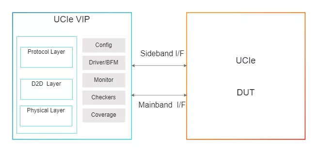
Best-in-Class UCIe Verification IP for your IP, SoC, and System-Level Design Testing The Cadence Verification IP (VIP) for Univer…
Best-in-Class UCIe Verification IP for your IP, SoC, and System-Level Design Testing
The Cadence Verification IP (VIP) for Universal Chiplet Interconnect Express (UCIe) is designed for easy integration in test benches at the IP, system-on-chip (SoC), and system level. The VIP for UCIe runs on all simulators and supports SystemVerilog along with the widely adopted Universal Verification Methodology (UVM). This enables verification teams to reduce the time spent on environment development and redirect it to cover a larger verification space, accelerate verification closure, and ensure end-product quality.
With a layered architecture and powerful callback mechanism, verification engineers can verify UCIe features at each functional layer (PHY, D2D, Protocol) and create highly targeted designs while taking advantage of the latest design methodologies for random testing to cover a larger verification space. The VIP for UCIe can be used as a standalone stack or layered with PCIe VIP.
Supported specifications: Universal Chiplet Interconnect Express Specification Version 1.1
Key Features
The following table describes key features from the specifications that are implemented in the VIP:
|
Feature Name |
Description |
|---|---|
|
UCIe 2.0 |
|
|
Protocol Layer Features |
|
|
D2D Adapter Layer Features |
|
|
PHY Features |
|
|
Interfaces |
|
|
Sideband Features |
|
|
Model Capabilities |
|
|
Monitor Mode |
|
|
Package |
|
|
Error Injections |
|
Note: some files may require an NDA depending on provider policy.

Simulation VIP for UCIE is a UCIe IP core from Cadence Design Systems, Inc. listed on Semi IP Hub.
Engineers should review the overview, key features, supported foundries and nodes, maturity, deliverables, and provider information before shortlisting this UCIe IP.
Yes. Buyers can compare this product with similar semiconductor IP cores or IP families based on category, provider, process options, and structured technical specifications.