Vendor: Cadence Design Systems, Inc. Category: DDR

Simulation VIP for DFI

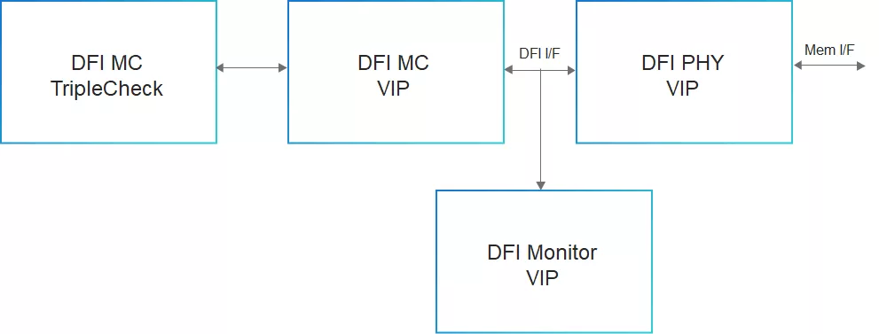
solution for extensive and fast verification used by multiple production designs.The Cadence® Verification IP (VIP) for DFI provi…

Overview

Complete solution for extensive and fast verification used by multiple production designs.

The Cadence® Verification IP (VIP) for DFI provides a mature, highly capable compliance verification solution for the DFI protocol. The VIP supports the simulation platform and enables metric-driven verification of IP and system-on-chip (SoC) designs against DFI protocol specifications. DFI VIP supports both the memory controller (MC) traffic generation and the PHY component, which samples from the DFI interface and drives to the memory interface for different memory variants. The VIP for DFI is compatible with the industry-standard Universal Verification Methodology (UVM) and supports all leading simulators.

Supported specification: DDR PHY Interface Specification v4.0, v5.0 and v5.1

Key features

  • DFI MC
  • Command Interface
    • Drives Command on different phases based on memory protocol requirement
    • DDR4-5, LPDDR4-5, HBM2E-3 and GDDR6-7
  • Command to Command Delay
    • Configurable different timing constraint requirements while driving a command through DFI interface for the memory
    • DDR4-5, LPDDR4-5, and HBM2E-3
  • Data Interface
    • Read and Write Data Interface
    • DDR4-5, LPDDR4-5, HBM2E-3 and GDDR6-7
  • Update Interface
    • MC-initiated and PHY initiated updates
    • DDR4-5, LPDDR4-5, HBM2E-3 and GDDR6-7
  • Training Interface
    • CA, Write, Write DQ, Read Training (Both MC initiated and PHY initiated)
    • DDR4, LPDDR4
  • PHY Master Interface
    • Supports PHY Master Interface
    • DDR4-5, LPDDR4-5, HBM2E-3 and GDDR6-7
  • WCK Interface
    • Supports WCK Interface
    • LPDDR5
  • Frequency Change Protocol
    • Initiates frequency change
    • DDR4-5, LPDDR4-5, and HBM2E-3
  • Low-Power Control
    • Initiates Low-Power Entry as per DFI5.0 and DFI4.0
    • DDR4-5, LPDDR4-5, HBM2E-3 and GDDR6-7
  • Data CS Gap
    • Data Path Chip Select Gap (Per Rank Delay line support)
    • DDR4-5, LPDDR4-5, and HBM2E-3
  • Refresh Command
    • Sends Refresh All and Refresh Per Bank command on every internal
    • DDR4-5, LPDDR4-5, and HBM2E-3
  • DFI Interactions
    • DFI Interaction Rules as per DFI 5.0
    • DDR5, LPDDR5, HBM3, GDDR6-7
  • 2N Mode
    • Command transmission in 2N Mode
    • DDR5
  • DBI and Data Mask
    • Generates Inverted/Masked Write Data and Invert received Read Data with dfi_rddata_dbi enabled
    • DDR4-5, LPDDR4-5, and HBM2E-3
  • CRC
    • Generates CRC and error injection
    • DDR4-5
  • Frequency Ratio
    • All possible frequency ratios as per specification
    • DDR4-5, LPDDR4-5, HBM2E-3 and GDDR6-7
  • GearDown Mode
    • Command transmission in GearDown Mode
    • DDR4
  • Checkers
    • Performs timing and protocol checks for signals driven by PHY
    • DDR4-5, LPDDR4-5, HBM2E-3 and GDDR6-7
  • Multi Channel Mode
    • Configurable Single/Multiple (Independent/Combine) Channel Interface
    • LPDDR4,HBM2E-3, GDDR6
  • RCK Interface
    • Enable/Disable Control on RCK signal for Read Transfer
    • GDDR7
  • DQE/DQX Interface
    • DQE/DQX Interface for CRC/7-8Bit encoding
    • GDDR7
  • CABI Interface
    • CABI interface for Command Inversion
    • GDDR6
  • Read Data EDC Interface
    • Sampling EDC signals with slice control using enable signal
    • GDDR
  • DFI PHY
  • Command Interface
    • Drives Command on different phases based on memory protocol requirement
    • DDR4-5, LPDDR4-5, HBM2E-3, GDDR6
  • Data Interface
    • Read and Write Data Interface
    • DDR4-5, LPDDR4-5, HBM2E-3, GDDR6
  • Update Interface
    • MC-initiated and PHY initiated updates
    • DDR4-5, LPDDR4-5, HBM2E-3, GDDR6
  • PHY Master Interface
    • Supports PHY Master Interface
    • DDR4-5, LPDDR4-5, HBM2E-3, GDDR6
  • WCK Interface
    • Supports WCK Interface
    • LPDDR5
  • Frequency Change Protocol
    • Initiates frequency change
    • LPDDR4-5, DDR4-5
  • Low-Power Control
    • Initiates Low-Power Entry as per DFI5.0 and DFI4.0
    • DDR4-5, LPDDR4-5, HBM2E-3, GDDR6
  • Data CS Gap
    • Data Path Chip Select Gap (Per Rank Delay line support)
    • LPDDR4-5, DDR4-5
  • DFI Interactions
    • DFI Interaction Rules as per DFI 5.0
    • LPDDR5,DDR4-5,HBM3
  • DBI and Data Mask
    • Generates Inverted/Masked Write Data and Invert received Read Data with dfi_rddata_dbi enabled
    • LPDDR4-5, DDR4-5,HBM3
  • Frequency Ratio
    • All possible frequency ratios as per specification
    • LPDDR4-5, DDR4-5,HBM2E-3, GDDR6
  • DRAM Interface
    • Supports DRAM interface as per required by DRAM
    • LPDDR4-5, DDR4-5, HBM2E-HBM3, GDDR6
  • Initialization/PHY Training
    • Fully configurable Initialization training for memory model, also PHY can initiate training independently through registers
    • LPDDR4-5, DDR4-5, HBM2E-HBM3, GDDR6
  • Run-time Configurations
    • PHY decodes MRW/MPC commands and auto-update its configuration, read-write latency based on that
    • LPDDR4-5, DDR4-5, HBM2E-HBM3, GDDR6
  • Multi-Rank
    • Supports Multi-Rank transfer interface
    • LPDDR4-5, DDR4-5
  • DBI
    • Generates inverted Write Data and inverted received Read Data if DBI is enabled in PHY
    • LPDDR4-5
  • ECC
    • Generates ECC for Write Data and check ECC for received Read Data ECC is enabled in PHY
    • LPDDR5
  • WCK
    • Supports Generation of WCK based on WCK:CK ratio
    • LPDDR5
  • CK
    • Supports Generation of DRAM clock based on frequency ratio
    • LPDDR4-5, DDR4-5, HBM2E-3, GDDR6
  • Training
    • Supports all the training required for DRAM
    • LPDDR4-5, DDR4-5, HBM2E-HBM3, GDDR6
  • CRC
    • Generation of CRC when PHY CRC Mode is on
    • DDR4-5
  • Dual Channel
    • Configurable Single/Dual (Independent/Combine) Channel Interface
    • LPDDR4
  • CABI Interface
    • CABI interface for Command Inversion
    • GDDR6
  • Read Data EDC Interface
    • Driving EDC signals with slice control using enable signal
    • GDDR6

Block Diagram

Files

Note: some files may require an NDA depending on provider policy.

Specifications

Identity

Part Number
Simulation VIP for DFI
Vendor
Cadence Design Systems, Inc.

Provider

Cadence Design Systems, Inc.
HQ: USA
If you want to achieve silicon success, let Cadence help you choose the right IP solution and capture its full value in your SoC design. Cadence® IP solutions offer the combined advantages of a high-quality portfolio, an open platform, a modern IP factory approach to quality, and a strong ecosystem. Now you can tackle IP-to-SoC development in a system context, focus your internal effort on differentiation, and leverage multi-function cores to do more, faster. The Cadence IP Portfolio includes silicon-proven Tensilica® IP cores, analog PHY interfaces, standards-based IP cores, verification IP cores, and other solutions as well as customization services for current and emerging industry standards. The Cadence IP Factory provides you with an automated approach to the customization, delivery, and verification of SoC IP. As a result, you can spend more time on differentiation, with the assurance that you'll meet your performance, power, and area requirements. Choosing Cadence IP enables you to design with confidence because you have more freedom to innovate your SoCs with less risk and faster time to market.

Learn more about DDR IP core

Which DDR SDRAM Memory to Use and When

This whitepaper provides an overview of the JEDEC memory standards to help SoC designers select the right memory solution, including IP, that best fits their application requirements.

Frequently asked questions about DDR Controller IP cores

What is Simulation VIP for DFI?

Simulation VIP for DFI is a DDR IP core from Cadence Design Systems, Inc. listed on Semi IP Hub.

How should engineers evaluate this DDR?

Engineers should review the overview, key features, supported foundries and nodes, maturity, deliverables, and provider information before shortlisting this DDR IP.

Can this semiconductor IP be compared with similar products?

Yes. Buyers can compare this product with similar semiconductor IP cores or IP families based on category, provider, process options, and structured technical specifications.

×
Semiconductor IP