Vendor: Cadence Design Systems, Inc. Category: DDR

Simulation VIP for DDR5

In production since 2014 on dozens of production designs.This Cadence® Verification IP (VIP) supports the JEDEC® Memory Device DD…

Overview

In production since 2014 on dozens of production designs.

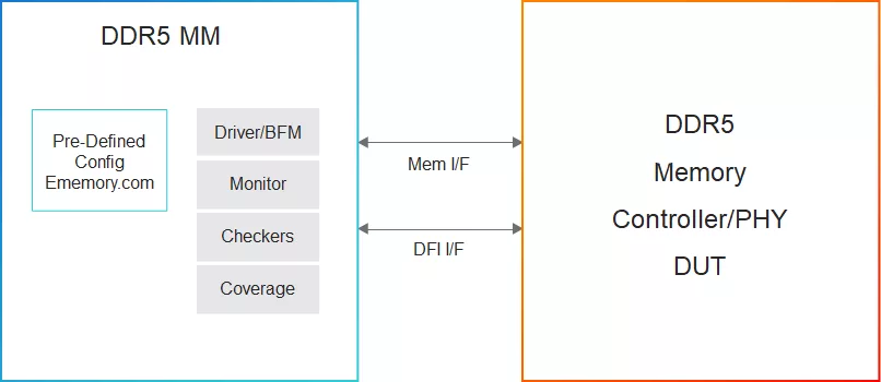
This Cadence® Verification IP (VIP) supports the JEDEC® Memory Device DDR5 SDRAM standard. It provides a highly capable compliance verification solution that supports simulation and formal analysis, making it applicable to intellectual property (IP), system-on-chip (SoC), and system-level verification. The VIP for DDR5 SDRAM is compatible with the industry-standard Universal Verification Methodology (UVM), runs on all leading simulators, and leverages the industry-standard Cadence Memory Model core architecture, interface, and use model.

The DDR5 standard is the next generation of DRAM device memory standard with many improvements in performance, reliability, and power saving over the previous generation of DRAM devices, DDR4. DDR5 addresses industry demand with increased bandwidth, capacity, power-saving features, and with more reliability through CRC and ECC.

Supported specification: JEDEC JESD79-5 specification.

Key features

  • Speeds
    • 3200, 3600, 4000, 4400, 4800, 5200, 5600, 6000, and 6400
  • Density
    • 8Gb, 16Gb, 24Gb, 32Gb, and 64Gb
  • Data Widths
    • x4, x8, and x16
  • Core DRAM Functionality
    • Reset and Initialization
    • Read/ Write and Write Pattern (All Burst Lengths including BL32, Type, Order)
    • Self Refresh, Power Down, and Maximum Power Saving Mode (MPSM)
    • Temperature Sensor (including support for Temperature Based Self Refresh)
    • Per Dram Addressability (PDA)
    • Write command features (tDQS2DQ Offset, Write Data Mask, twr timing changes, etc.)
  • Training Modes
    • Training Modes (Read Training Pattern, Read Preamble Training Mode, CATM, CSTM, VrefCS, VrefCA, Internal and External Write Leveling Training Mode, etc.)
    • ZQ Calibration Commands
    • DQS Interval Oscillator
  • Commands
    • Support of all DDR5 JEDEC Spec defined Commands: MRW, MRR, ACT, WrP, WrPA, Wr, WrA, Rd, RdA, VrefCA, VrefCS, RFM, REF, SRE, SREF, PDE, PDX, MPC, and PRE
  • Signal Integrity and Routing
    • Post Package Repair (PPR)
    • On-Die Termination (ODT)
    • CA_ODT Strap Operation
    • CAI, MIR, CA_ODT Pin Support
    • Loopback Mode
  • DRAM Timings
    • Timing Parameters by Speed Grades, e.g., bus timings (setup, hold, pulse width checks)
    • Command Spacing checks
    • DDR5 timings rounding algorithm
  • Data Integrity
    • ECC and ECS Modes
    • CRC generator and checks
  • Command Decoding
    • Single-cycle and two-cycle commands with support for both targeted and non-targeted commands
    • 1N and 2N Mode support
  • Programmable Configurations
    • Programmable Pre/post and Interamble, CL/CWL, /tdllk/tccdl/dllreset
  • Bank Groups
    • Supports 8 or 4 bank groups
    • Modeling the concept and the timing associated with back-to-back access to the same and different bank groups
  • Refresh Options
    • Normal 1X Refresh Mode and Fine Granularity 2X Refresh Mode
    • 1X Refresh Rate, 2X Refresh Rate
  • Additional Features
    • Support of Board Delays for All the Pins
    • Support for Inter Rank ODT and Command Spacing Checks
    • Support for Active Byte Lane Mask for X16 device
  • Verification Flows
    • Query Select Verification Flow
    • Random Config Verification Flow

Block Diagram

Files

Note: some files may require an NDA depending on provider policy.

Specifications

Identity

Part Number
Simulation VIP for DDR5
Vendor
Cadence Design Systems, Inc.

Provider

Cadence Design Systems, Inc.
HQ: USA
If you want to achieve silicon success, let Cadence help you choose the right IP solution and capture its full value in your SoC design. Cadence® IP solutions offer the combined advantages of a high-quality portfolio, an open platform, a modern IP factory approach to quality, and a strong ecosystem. Now you can tackle IP-to-SoC development in a system context, focus your internal effort on differentiation, and leverage multi-function cores to do more, faster. The Cadence IP Portfolio includes silicon-proven Tensilica® IP cores, analog PHY interfaces, standards-based IP cores, verification IP cores, and other solutions as well as customization services for current and emerging industry standards. The Cadence IP Factory provides you with an automated approach to the customization, delivery, and verification of SoC IP. As a result, you can spend more time on differentiation, with the assurance that you'll meet your performance, power, and area requirements. Choosing Cadence IP enables you to design with confidence because you have more freedom to innovate your SoCs with less risk and faster time to market.

Learn more about DDR IP core

Which DDR SDRAM Memory to Use and When

This whitepaper provides an overview of the JEDEC memory standards to help SoC designers select the right memory solution, including IP, that best fits their application requirements.

Frequently asked questions about DDR Controller IP cores

What is Simulation VIP for DDR5?

Simulation VIP for DDR5 is a DDR IP core from Cadence Design Systems, Inc. listed on Semi IP Hub.

How should engineers evaluate this DDR?

Engineers should review the overview, key features, supported foundries and nodes, maturity, deliverables, and provider information before shortlisting this DDR IP.

Can this semiconductor IP be compared with similar products?

Yes. Buyers can compare this product with similar semiconductor IP cores or IP families based on category, provider, process options, and structured technical specifications.

×
Semiconductor IP