Vendor: Eureka Technology, Inc. Category: SD / eMMC Controller

SD/SDIO 2.0 MMC Host Controller

The EP550 is a host controller for SD memory card, SDIO and MMC interface.

Overview

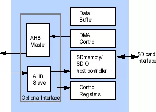
The EP550 is a host controller for SD memory card, SDIO and MMC interface. The core connects the host CPU of the system to the SD card socket. External SD cards can be accessed by the host CPU through the EP550 controller core IP.

SD memory and SDIO are low cost, high speed interfaces designed for removable mass storage and IO devices. It is a very flexible architecture supporting variable clock rate from 0 to 25Mhz and data width of 1 to 4 bits. A data rate of up to 12.5Mbyte/sec (100Mbs) can be realized with SD interface. Features such as plug and play, auto-detection, error correction, write protection are standard with SD card interface.

The EP550 SD card host controller core is designed according to the SD Association’s SD host controller specification. The core presents a very simple view of the SD card to the system software. All access to the SD card are made through the standard control register set. DMA, burst access, CRC error detection, interrupt, timing, etc. are supported by the controller core. Because of the standard register set, the EP550 can be used to replace other existing SD controllers with no change to system software.

There are several options for user hardware interface to the controller core. The controller supports generic user interface optimized for on-chip logic interface as well as embedded CPU interface such as AMBA AHB bus. To access the SD card, the host CPU simply issue read/write access to the control registers in the core. The controllers core handles all the SD card protocol automatically including data shifting, timing and CRC generation. The core has a built-in DMA controller so that data can be automatically transferred between the system and the SD card without CPU intervention.

With the EP550, SD card interface can be realized with very little development cost. Designer can add SD memory and SDIO interface to the system by simply adding the EP550 module without changing the rest of the system architecture.

Key features

  • Host controller for SDIO, SD memory card, and MMC interface.
  • Allows host CPU to access SD and MMC devices.
  • Simple user interface optimized for on-chip bus connection.
  • User interface supports 32-bit and 64-bit data.
  • Option to integrate with other CPU bus slaves to support direct access by various CPU’s including PowerPC, MPC860, ARM, SH2/3/4, MIPS, and ARC microprocessors.
  • Supports SDIO DMA operation for high speed data transfer.
  • Supports SD host controller standard register set.
  • Fully programmable access timing.
  • Supports multi-function SD cards, command suspend, resume, and block transfers.
  • Option to operate the user interface and card interface at different clock domains.
  • Direct mapping of host address space to card address space.
  • Designed for ASIC and FPGA implementations.
  • Fully static design with edge triggered flip-flops.

Block Diagram

Files

Note: some files may require an NDA depending on provider policy.

Specifications

Identity

Part Number
EP550
Vendor
Eureka Technology, Inc.

Provider

Eureka Technology, Inc.
HQ: USA
Eureka Technology Inc. provides reusable IP cores for ASIC, PLD and system designs. These system level function cores are designed to:
  • Shorten Time-to-market
  • Eliminate Design Risks
  • Reduce Development Costs
As today's technologies evolve in a very fast pace, design engineers are constantly looking for ways to speed up the design cycle in order to have product in the market ahead of the competitions. The use of reusable IP cores in IC and system design has emerged as the methodology of choice to address the needs for rapid productization, fast prototyping and software/hardware co-development. Eureka Technology help design engineers stay in the forefront of this new design methodology by providing reusable IP cores. Our reusable IP cores are silicon proven and pre-verified to meet and exceed customer requirements. Design risk is virtually eliminated since each one of these cores has been fully tested and proven in real world applications. Since founded in 1993, Eureka Technology has established itself as a leading reusable IP core provider with customer base in the United States, Japan, and Europe. We have provided reusable IP cores to many market leaders in the computer, electronics and semiconductor industries. Our technologies have been incorporated into tens of million dollars' worth of products sold by our customers. We also have entered partnership agreements with leading silicon vendors to incorporate our reusable IP cores into their silicon products. However, our important partnership is the one with our customers and we would like to be the design partner for your next project.

Learn more about SD / eMMC Controller IP core

Types of Storages for Computing System-On-Chips

We are living in an age where we generate the same amount of data each year that has been generated since antiquity. Ever wondered how and where these peta /exa/zetta bytes of data are stored?

Virtual Prototyping Platform with Flash Memory

In this paper we will see how the flash memories developed using Carbon Model Studio helps to bring up an ARM® Cortex A7 flash memory sub-system with primary and secondary boot codes. Flash memories system demonstrated here can be used for early boot code and driver development for any CPU based SoC.

UFS Goes Mainstream

UniversalFlash Storage (UFS) was created for mobile applications and computer systems requiring high performance and low power consumption. These systems typically use embedded Flash based on the JEDEC standard eMMC. UFS was defined by JEDEC as the evolutionary replacement for eMMC offering significantly higher memory bandwidth. The standard builds on existing standards such as the SCSI command set, the MIPI Alliance M-PHY and UniPro as well as eMMC form factors to simplify adoption and development.

Universal Flash Storage: Mobilize Your Data

Universal Flash Storage (UFS) was created for mobile applications and computer systems requiring high performance and low power consumption. These systems typically use embedded Flash based on the JEDEC standard eMMC. UFS was defined by JEDEC as the evolutionary replacement for eMMC offering significantly higher memory bandwidth. The standard builds on existing standards such as the SCSI command set, the MIPI Alliance M-PHY and UniProSM as well as eMMC form factors to simplify adoption and development.

Frequently asked questions about SD / eMMC Controller IP cores

What is SD/SDIO 2.0 MMC Host Controller?

SD/SDIO 2.0 MMC Host Controller is a SD / eMMC Controller IP core from Eureka Technology, Inc. listed on Semi IP Hub.

How should engineers evaluate this SD / eMMC Controller?

Engineers should review the overview, key features, supported foundries and nodes, maturity, deliverables, and provider information before shortlisting this SD / eMMC Controller IP.

Can this semiconductor IP be compared with similar products?

Yes. Buyers can compare this product with similar semiconductor IP cores or IP families based on category, provider, process options, and structured technical specifications.

×
Semiconductor IP