Types of Storages for Computing System-On-Chips
We are living in an age where we generate the same amount of data each year that has been generated since antiquity. Ever wondered how and where these peta /exa/zetta bytes of data are stored?
A compact low power and scalable IP core which provides a simple, firmware-friendly cost-effective Physical Link interface for me…
A compact low power and scalable IP core which provides a simple, firmware-friendly cost-effective Physical Link interface for memory, i/o and combo devices, such as SD-based memory cards, Mini SD, Micro SD, SDIO Bluetooth devices, SDIO GPS, etc.
The SD/SDIO Device IP core is designed for an easy integration with any card controller and any system bus, with minimum firmware development overhead.
An optional data buffer extension module is provided in order to improve CPU utilization, e.g. for performance-sensitive systems. An internal DMA engine gives further CPU off load capability.
The power and area are key factors throughout the design, ensuring a real cost-effective solution for SD based products.
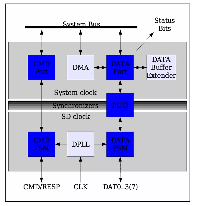
ARCHITECTURE
The front end of the core implements a SD Physical Link as defined by SD specifications for 1 / 4 (/8) data lines and for SPI interface. At its back end the core interfaces to the system controller through a generic 8 bit bus based on Wishbone specifications.
Command Channel
The CommandChannelconsists of a CommandPort and a Command FSM. The Command Port provides a programing interface for accepting commands and sending back responses. The control and status signals are synchronized and connected to the Command FSM, which resides in the SD clock domain. The following activities are done within the context of the Command FSM: serializing and de serializing the commands over the SD command line, CRC7 check for incoming commands, CRC7 calculation for outgoing responses, command/response related errors and status report, controlling busy signal after responses, SPI mode recognition.
Data Channel
The Data Port together with the Data FSM build up the Data Channel portion. The Data Port provides a programing interface for receiving write data sent by the host following write commands, and for sending data to the host in response to read commands. The SD physical data interface supports 1 and 4 (optional: 8) lines of data. Following a read command, the system controller starts writing data bytes to the Data Port. The data are manipulated and sent over the physical lines by the data FSM. CRC16 checksum is added at the end of each block. In the reverse way, following a write command, the data FSM collects bits from the physical interface, packs them into bytes and pushes the bytes into the FIFO. The system controller in turn reads the new data through the Data Port. System resources can be better utilized with the buffer extension module which stores the data blocks during the data FSM read/write operations, thereby providing an additional system controller and bus offload.
DMA (Optional)
The DMA engine can be programmed to transfer data between a specified locations on the system bus address space and the Data Port FIFO, in both directions (receive and send).
Synchronization
The front end of the core consists of command and data state machines driven by SD clock. The back end consists the programing interface entities (Command Port and Data Port) and is driven by the same clock domain of the system bus. The control and status signals that cross the two clock domains are synchronized using 2-flop based paradigm, while the data are synchronized using a Dual-port FIFO.
Note: some files may require an NDA depending on provider policy.

SD/SDIO Device IP Core is a SD / eMMC Controller IP core from ASICS World Services, LTD. listed on Semi IP Hub.
Engineers should review the overview, key features, supported foundries and nodes, maturity, deliverables, and provider information before shortlisting this SD / eMMC Controller IP.
Yes. Buyers can compare this product with similar semiconductor IP cores or IP families based on category, provider, process options, and structured technical specifications.