Vendor: ASICS World Services, LTD. Category: SD / eMMC Controller

SD/SDIO/MMC Host Controller

A , easy to integrate and cost-effective IP core featuring SD/SDIO/MMC Host Controller Interface for SoC/PDA applications that co…

Overview

A complete, easy to integrate and cost-effective IP core featuring SD/SDIO/MMC Host Controller Interface for SoC/PDA applications that connect to SD/MMC memory cards, SDIO/combo devices such as Bluetooth and GPS, or CEATA devices.

The SD/SDIO/MMC IP Core can smoothly integrate to any host system using one of the slave interfaces listed above. Mapping the card memory on the system bus address space dramatically reduces the overhead of firmware and software development required for embedding the core. The implementation of retry and interrupt-on completion mechanism minimizes the utilization of system resources, such as bus or cpu cycles. These key features speed up the time-to-market, making the core a real cost-effective solution for SoC and PDA developers.
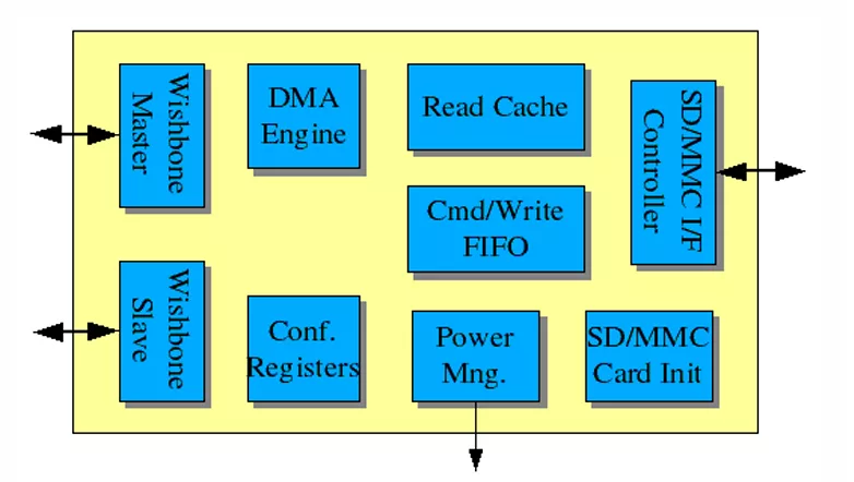
ARCHITECTURE

The core can be divided into 3 main functions: command/write channel, read channel and configuration and management channel. The command/write path consists of a command builder, command/write FIFO, CRC generation, completion and interrupt handling. The read path contains a read cache with a configurable page size and up to 8 valid pages in cache. It also consists of CRC checking and error handling logics. The configuration and management channel provides access to the core control and status registers. The core also provides the host with clock control interface and LED outputs.

SD/MMC Host Physical Layer Interface

The core front-end supports SD protocol in 1bit and 4bit modes, MMC protocol and SPI. Its' functional blocks include command execution and response interpretation, data write and read FSM, CRC generators, SD/MMC/SPI identification, interrupting the host upon events such as card insertion/removal, completion of command execution, completion of page update in the cache, error detection and more. Reliability is achieved through completion and error indications.

Host Bus Interface

A SD/MMC card is mapped on the host address space, such that the implementation is virtually transparent to the host. Write data is gathered and packed into write blocks. Read access may be followed by immediate data if the address is valid in the read cache (cache-hit), or it may initiate a data page replacement if the address is not valid in the cache (cache-miss).

Internal Buffers

The SD/MMC Host IP Core deploys two buffering entities: command/write FIFO and read cache. The core can be provided with a variety of buffering space, e.g. 512 byte, 1K byte, 2K byte or 4K byte. Moreover, buffering space can be assigned optimally according to system demands. E.g., applications designed solely for read-only cards may have the majority of buffer space allocated to their read cache and minimal buffer space allocated to their write FIFO, whereas applications designed for writing and reading data may have a balanced buffer allocation. SDIO applications that don't require memory access support may use minimal buffering for both read and write path, thereby reducing the overall SoC area.

Key features

  • Compliant with SD Spec ver1.01/1.10 and  MultiMediaCard Spec ver4.X/3.X
  •  Supports SD/MMC 1bit/4bit/8bit modes, as well as  SPI mode
  •  Supports MMCplus and MMCmobile specifications
  •  Supports CEATA specifications (ver1.0), including
  •  Completion Signal logic
  •  Provides memory-mapped and i/o access to
  •  SD/MMC cards through a Wishbone slave adapter
  •  Supports all command classes, including MMCA
  •  stream write and read
  •  Internal DMA engine
  •  Read cache with variable physical size and configurable page size to boost-up card read access  performance.
  •  Interrupt-on-completion handshake eliminates  host resources utilization during read operations
  •  Write FIFO with variable size and configurable   thresholds to enable non-blocking operations and  to prevent back-pressure propagation from card to  host
  •  Supports posted write operations
  •  Supports SDIO IRQ signaling
  •  Implements multi-block read and write commands  with internal STOP command generation (CMD12)  for enhanced throughput
  •  Supports any data block length
  •  Supports fast and slow SD cards. SD clock  frequency: 0-50+MHz
  •  Supports hot card insertion and removal
  •  SD/SDIO/MMC/SPI identification flow done by  hardware
  •  Provides command port interface for direct access   to the SD/MMCdevices and for I/O access to SDIO  devices
  •  Internal implementation of CRC16 for data lines  and CRC7 for command line
  •  Wide range of configuration options to fine-tune   the core according to the system specifications and  demands
  •  Wide range of maskable interrupt events, such as  card detection, block transfer termination,  command completion, error detection end many  more
  •  Slave System Interface:
    •  WISHBONE  
    • AMBA 
    • CoreConnect
    •  AVALON
    •  Customer specified bus interface
  •  No dedicated local memory required
  •  Compact and cost-effective solution for SoC and  PDA

Block Diagram

Benefits

  • Flexible
  • Compact
  • Cost-effective

What’s Included?

  • Verilog Source Code
  • Test Bench
  • Sample Syntheis scripts
  • Dcumentation

Files

Note: some files may require an NDA depending on provider policy.

Specifications

Identity

Part Number
SD_MMC_HOST1
Vendor
ASICS World Services, LTD.

Provider

ASICS World Services, LTD.
ASICs World Services specialize in providing top-notch IP Cores and design services. We will assist you in any phase of the design cycle, or take your idea from the conceptual stage to final product. With over 60 years of experience in the field, we have a long list of successfully completed projects.

Learn more about SD / eMMC Controller IP core

Types of Storages for Computing System-On-Chips

We are living in an age where we generate the same amount of data each year that has been generated since antiquity. Ever wondered how and where these peta /exa/zetta bytes of data are stored?

Virtual Prototyping Platform with Flash Memory

In this paper we will see how the flash memories developed using Carbon Model Studio helps to bring up an ARM® Cortex A7 flash memory sub-system with primary and secondary boot codes. Flash memories system demonstrated here can be used for early boot code and driver development for any CPU based SoC.

UFS Goes Mainstream

UniversalFlash Storage (UFS) was created for mobile applications and computer systems requiring high performance and low power consumption. These systems typically use embedded Flash based on the JEDEC standard eMMC. UFS was defined by JEDEC as the evolutionary replacement for eMMC offering significantly higher memory bandwidth. The standard builds on existing standards such as the SCSI command set, the MIPI Alliance M-PHY and UniPro as well as eMMC form factors to simplify adoption and development.

Universal Flash Storage: Mobilize Your Data

Universal Flash Storage (UFS) was created for mobile applications and computer systems requiring high performance and low power consumption. These systems typically use embedded Flash based on the JEDEC standard eMMC. UFS was defined by JEDEC as the evolutionary replacement for eMMC offering significantly higher memory bandwidth. The standard builds on existing standards such as the SCSI command set, the MIPI Alliance M-PHY and UniProSM as well as eMMC form factors to simplify adoption and development.

Frequently asked questions about SD / eMMC Controller IP cores

What is SD/SDIO/MMC Host Controller?

SD/SDIO/MMC Host Controller is a SD / eMMC Controller IP core from ASICS World Services, LTD. listed on Semi IP Hub.

How should engineers evaluate this SD / eMMC Controller?

Engineers should review the overview, key features, supported foundries and nodes, maturity, deliverables, and provider information before shortlisting this SD / eMMC Controller IP.

Can this semiconductor IP be compared with similar products?

Yes. Buyers can compare this product with similar semiconductor IP cores or IP families based on category, provider, process options, and structured technical specifications.

×
Semiconductor IP