Overview
The High Speed Synchronous Serial Interface (HSI) Controller is used to provide high bandwidth, point-to-point, serial communication between two peers, like the cellular modem and application processor on a mobile platform, such as a smartphone or a tablet. The HSI Controller IP is designed to provide MIPI HSI 1.00 compliant connectivity to a SoC.
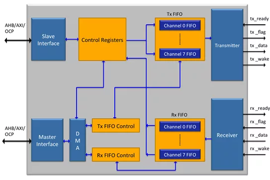
Three variations of the IP are currently available with support for AHB, AXI or OCP system buses. The HSI Controller’s internal registers are accessible through programmed IO transactions, in which case the IP functions as a bus slave. All data transfers between the SoC’s system memory and HSI interface happen either in PIO mode or in DMA mode as programmed by the driver/firmware.
All data received from system memory is held in the transmit FIFO and output as serial data over the HSI physical interface. Conversely, all serial data received from the HSI interface is captured in the receive FIFO before it is sent to the system memory. The FIFO’s and their associated logic can be structured with up to 8 logical channels, each with configurable depth.
Learn more about UniPro IP core
UniversalFlash Storage (UFS) was created for mobile applications and computer systems requiring high performance and low power consumption. These systems typically use embedded Flash based on the JEDEC standard eMMC. UFS was defined by JEDEC as the evolutionary replacement for eMMC offering significantly higher memory bandwidth. The standard builds on existing standards such as the SCSI command set, the MIPI Alliance M-PHY and UniPro as well as eMMC form factors to simplify adoption and development.
Universal Flash Storage (UFS) was created for mobile applications and computer systems requiring high performance and low power consumption. These systems typically use embedded Flash based on the JEDEC standard eMMC. UFS was defined by JEDEC as the evolutionary replacement for eMMC offering significantly higher memory bandwidth. The standard builds on existing standards such as the SCSI command set, the MIPI Alliance M-PHY and UniProSM as well as eMMC form factors to simplify adoption and development.
The emerging MIPI standards are designed to ensure interoperability among devices and software that are used in products for the exploding hand-held market. The standards facilitate the interconnection of multiple, mixed-signal integrated circuit devices on a single hand-held product. Use of the standards ensures low power, low pin count and interoperability of all the devices in the system and easy integration.
Divyang Mali