UCIe D2D Adapter Explained: Architecture, Flit Mapping, Reliability, and Protocol Multiplexing
Understand the role of the UCIe D2D Adapter in enabling reliable, scalable, multi-protocol die-to-die communication for chiplet architectures.
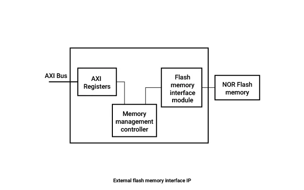
Flash memory forms a basic constituent in many FPGA based embedded systems using Xilinx SRAM based FPGAs.
Note: some files may require an NDA depending on provider policy.

External Flash Memory Interface IP is a Protocol Bridge IP core from Faststream Technologies listed on Semi IP Hub.
Engineers should review the overview, key features, supported foundries and nodes, maturity, deliverables, and provider information before shortlisting this Protocol Bridge IP.
Yes. Buyers can compare this product with similar semiconductor IP cores or IP families based on category, provider, process options, and structured technical specifications.