Vendor:
Cadence Design Systems, Inc.
Category:
UltraLink
40G UltraLink D2D PHY
High-performance, low-latency PHY for D2D connectivity The UltraLink™ Die-to-Die (D2D) PHY enables SoC providers to deliver more …
Overview
High-performance, low-latency PHY for D2D connectivity
The UltraLink™ Die-to-Die (D2D) PHY enables SoC providers to deliver more customized solutions that offer higher performance and yields while also shortening development cycles and reducing costs through greater IP reuse.
It is a mature solution that is silicon proven in multiple foundries and different process nodes.
Key features
- Innovative mixed-signal architecture to achieve high bandwidth, ultra low latency and low power
- Flexible data rate from 20Gbps to 40Gbps
- Built-in self-test features to ensure “known good die”
- Interoperable between different technology nodes and foundries
- Easy routing and straightforward integration
- Achieves better than 10-15 bit error rate (BER) without requiring forward error correction (FEC)
- Integrated scrambling and lane de-skew functionality
- Supports -40ºC to 125ºC industrial temperature range
Block Diagram
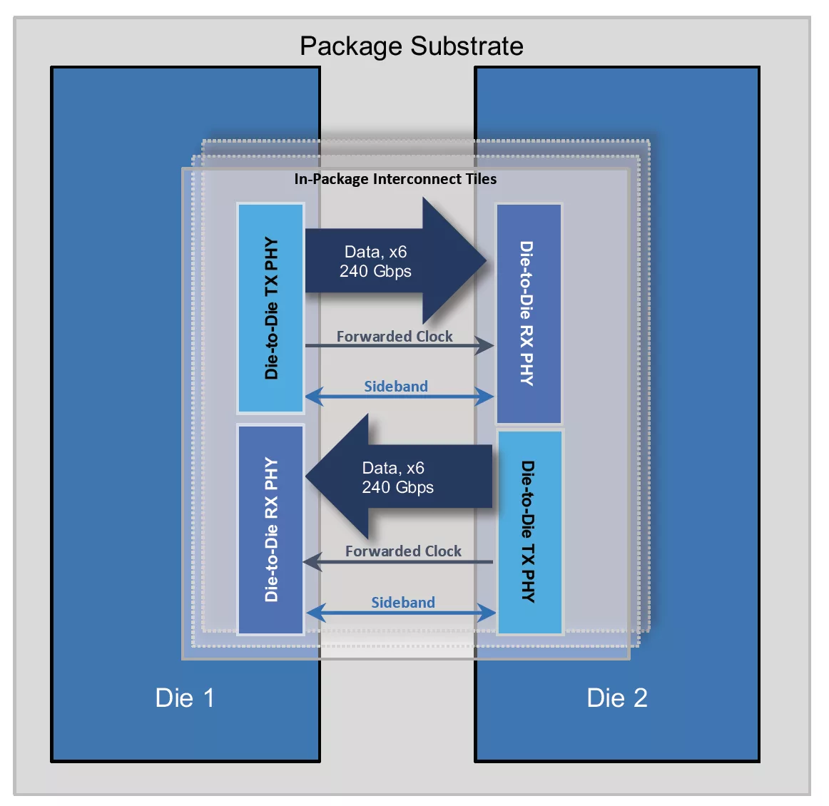
40G UltraLink D2D PHY block diagram
Applications
- High Performance Compute,
- AI,
- ML,
- Servers,
- Networking,
- Communications,
- Consumer Electronics,
- Data Processing,
- Industrial and Medical,
- Military/Civil Aerospace
What’s Included?
- Integration views: LEF abstract, timing views (.LIB), Verilog behavioral model, gate-level netlist, SDF, DRC, LVS, ANT reports, and GDSII layout and layer map
- Verilog testbench with example run scripts, demonstration tests, and bus functional models
- Full documentation set including integration, user, and programmer guides
- DFT collateral including ATPG generation and setup guidelines and scan abstracts (CTL), High Volume Manufacturing (HVM) kit
- IPXACT register abstracts, IBIS-AMI kit
Files
Note: some files may require an NDA depending on provider policy.
Silicon Options
| Foundry | Node | Process | Maturity |
|---|---|---|---|
| GlobalFoundries | 12nm | LP | Silicon Proven |
Specifications
Identity
Part Number
40G UltraLink D2D PHY
Vendor
Cadence Design Systems, Inc.
Provider

Cadence Design Systems, Inc.
HQ:
USA
If you want to achieve silicon success, let Cadence help you choose the right IP solution and capture its full value in your SoC design. Cadence® IP solutions offer the combined advantages of a high-quality portfolio, an open platform, a modern IP factory approach to quality, and a strong ecosystem.
Now you can tackle IP-to-SoC development in a system context, focus your internal effort on differentiation, and leverage multi-function cores to do more, faster.
The Cadence IP Portfolio includes silicon-proven Tensilica® IP cores, analog PHY interfaces, standards-based IP cores, verification IP cores, and other solutions as well as customization services for current and emerging industry standards. The Cadence IP Factory provides you with an automated approach to the customization, delivery, and verification of SoC IP. As a result, you can spend more time on differentiation, with the assurance that you'll meet your performance, power, and area requirements.
Choosing Cadence IP enables you to design with confidence because you have more freedom to innovate your SoCs with less risk and faster time to market.
Learn more about UltraLink IP core
Frequently asked questions about UltraLink IP cores
What is 40G UltraLink D2D PHY?
40G UltraLink D2D PHY is a UltraLink IP core from Cadence Design Systems, Inc. listed on Semi IP Hub. It is listed with support for globalfoundries Silicon Proven.
How should engineers evaluate this UltraLink?
Engineers should review the overview, key features, supported foundries and nodes, maturity, deliverables, and provider information before shortlisting this UltraLink IP.
Can this semiconductor IP be compared with similar products?
Yes. Buyers can compare this product with similar semiconductor IP cores or IP families based on category, provider, process options, and structured technical specifications.