GLOBALFOUNDRIES Demonstrates 3D TSV Capabilities on 20nm Technology
Fab 8 in New York delivers functional 20nm silicon with Through-Silicon-Vias (TSVs)
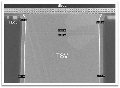
Milpitas, Calif., April 2, 2013 – GLOBALFOUNDRIES todayannounced the accomplishment of a key milestone in its strategy to enable 3D stacking of chips for next-generation mobile and consumer applications. At its Fab 8 campus in Saratoga County, N.Y., the company has demonstrated its first functional 20nm silicon wafers with integrated Through-Silicon Vias (TSVs). Manufactured using GLOBALFOUNDRIES' leading-edge 20nm-LPM process technology, the TSV capabilities will allow customers to stack multiple chips on top of each other, providing another avenue for delivering the demanding performance, power, and bandwidth requirements of today's electronic devices.
TSVs are vertical vias etched in a silicon wafer that are filled with a conducting material, enabling communication between vertically stacked integrated circuits. The adoption of three-dimensional (3D) chip stacking is increasingly being viewed as an alternative to traditional technology node scaling at the transistor level. However, TSVs present a number of new challenges to semiconductor manufacturers.
GLOBALFOUNDRIES utilizes a “via-middle” approach to TSV integration, inserting the TSVs into the silicon after the wafers have completed the Front End of the Line (FEOL) flow and prior to starting the Back End of the Line (BEOL) process. This approach avoids the high temperatures of the FEOL manufacturing process, allowing the use of copper as the TSV fill material. To overcome the challenges associated with the migration of TSV technology from 28nm to 20nm, GLOBALFOUNDRIES engineers have developed a proprietary contact protection scheme. This scheme enabled the company to integrate the TSVs with minimal disruption to the 20nm-LPM platform technology, demonstrating SRAM functionality with critical device characteristics in line with those of standard 20nm-LPM silicon.
“Our industry has been talking about the promise of 3D chip stacking for years, but this development is another sign that the promise will soon be a reality,” said David McCann, vice president of packaging R&D at GLOBALFOUNDRIES. “Our next step is to leverage Fab 8's advanced TSV capabilities in conjunction with our OSAT partners to assemble and qualify 3D test vehicles for our open supply chain model, providing customers with the flexibility to choose their preferred back-end supply chain.”
As the fabless-foundry business model evolves to address the realities of today's dynamic market, foundries are taking on increasing responsibility for managing the supply chain to deliver end-to-end solutions that meet the requirements of the broad range of leading-edge designs. To help address these challenges, GLOBALFOUNDRIES is engaging early with partners to jointly develop solutions that will enable the next wave of innovation in the industry. This open and collaborative approach will give customers maximum choice and flexibility, while delivering cost savings, faster time-to-volume, and a reduction in the technical risk associated with developing new technologies.

ABOUT GLOBALFOUNDRIES
GLOBALFOUNDRIES is the world's first full-service semiconductor foundry with a truly global footprint. Launched in March 2009, the company has quickly achieved scale as the second largest foundry in the world, providing a unique combination of advanced technology and manufacturing to more than 160 customers. With operations in Singapore, Germany and the United States, GLOBALFOUNDRIES is the only foundry that offers the flexibility and security of manufacturing centers spanning three continents. The company's three 300mm fabs and five 200mm fabs provide the full range of process technologies from mainstream to the leading edge. This global manufacturing footprint is supported by major facilities for research, development and design enablement located near hubs of semiconductor activity in the United States, Europe and Asia. GLOBALFOUNDRIES is owned by the Advanced Technology Investment Company (ATIC). For more information, visit http://www.globalfoundries.com.
Related Semiconductor IP
- 6-bit, 12 GSPS Flash ADC - GlobalFoundries 22nm
- All Digital Fractional-N RF Frequency Synthesizer PLL in GlobalFoundries 22FDX
- eFPGA on GlobalFoundries GF12LP
- ADPLL 2GHz Clock Generator - GLOBALFOUNDRIES 22FDX
- MIPI C/D Combo PHY RX - GlobalFoundries 22FDX
Related News
- GLOBALFOUNDRIES Fab 8 Adds Tools To Enable 3D Chip Stacking at 20nm and Beyond
- UMC Aligns With IBM on 20nm Process with FinFET 3D Transistors
- TSMC Announces Move to 20nm Process
- Toppan Completes 22nm and 20nm Production Photomask Process through Toppan-IBM Joint Development
Latest News
- Lattice Collaborates with TI to Accelerate Edge AI for Robotics and Industrial Applications
- Alchip Appoints Freddy Engineer Chief Business Officer and North America General Manager
- Perceptia Devices and Dolphin Semiconductor Partner to Deliver Best-in-Class IP Portfolio Covering Power Management, Clocking, High-Quality Audio and In-Situ Monitoring
- TSMC Chases Soaring AI Demand
- EU DARE Project Is Scrambling to Replace Codasip