Vendor: Beyond Semiconductor Category: DDR

SDRAM/SRAM/FLASH Memory Controller

Increasing SoC/ASIC devices' complexity also demands increase in memory bandwidth.

Overview

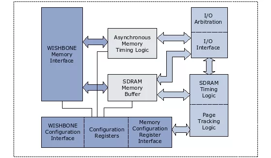
Increasing SoC/ASIC devices' complexity also demands increase in memory bandwidth. Single data rate devices are being replaced by double (and more) data rate devices in applications where memory bandwidth is essential. The development trend in DDR SDRAM devices is biased towards higher clock frequencies and higher latencies. Beyond DDR SDRAM Memory Controller IP Core was developed with this trend in mind. It interleaves accesses when possible, maximizing utilization of memory control and data buses. This reduces overall memory access latencies while utilizing its higher bandwidth capabilities.
Beyond DDR SDRAM Memory Controller IP Core provides access to external synchronous dynamic memory devices for SoC designs using WISHBONE SoC interconnect bus as internal bus. A wide variety of different memory device organizations and speeds are supported. Beyond DDR SDRAM Memory Controller IP Core also uses a lot of optional, compile time parameters, which makes it configurable for use in a wide variety of applications.
 

Key features

  • Memory Interface
    • Compile time configurable number of chip select signals – two to four
    • Software programmable chip select address range for each chip select – 8MB to 4GB
    • Compile time configurable memory data bus width. Supported 16, 32 and 64 bits
    • Utilization of write data mask signals for incomplete write bursts
    • Compile time configurable memory address bus width
    • Standard DDR-SDRAM control interface
    • External control signals for standard asynchronous static devices
    • Software configurable external memory device data width for each chip select
    • Supported widths are 8, 16, 32 and 64 bits for SDRAM devices and 8, 16 and 32 for asynchronous devices
    • Register interface for software initiated SDRAM initialization sequence
    • Support for asynchronous page mode static devices
    • Possible SDRAM burst sizes are 1, 2, 4 and 8
    • Software programmable asynchronous static memory device timing parameters for every chip select
    • Software programmable SDRAM memory device timings
    • Software programmable SDRAM memory organization
    • Additional DDR2 SDRAM control interface
    • Independent of data transmit and capture implementation
    • Pipelined, out-of-order memory command generation. Number of pipeline stages is selected at compile time according to application needs
    • Automatic SDRAM refresh generation
    • Register interface for software initialization and suspension of external memory devices
    • Page tracking logic implemented to reduce access latencies. Tracked number of pages is selected at compile time according to application needs
  • Wishbone Interface
    • Beyond DDR SDRAM Memory Controller IP Core implements four WISHBONE Rev. B.3 compliant slave interfaces to serve memory access requests
    • All WISHBONE burst, classic and single transfer cycles are supported for write and read operations
    • WISHBONE burst operations are taken advantage of to increase memory and WISHBONE buses utilization
    • Each memory access WISHBONE port can be configured at compile time to support either 32 or 64 bit data width
    • The fifth WISHBONE Slave interface is fixed at 32 bit width and is used for core, external memory devices and physical layer configuration
  • Core Internals
    • The core can run memory interface at any integer multiple frequency of that at WISHBONE bus
    • The core's implementation provides compile time parameters to configure control and data paths. This makes it possible to configure a core in a manner that matches total memory bandwidth with total WISHBONE bandwidth
    • Single control/data path implementation: all memory access arbitration is done at WISHBONE ports' side, single write data and read data paths are implemented. For applications with lowest bandwidth requirements
    • Double control/data path implementation: two to one arbitration is done at WISHBONE ports' side as well as at memory timing interface's side. For applications with balanced bandwidth requirements
    • Quad control/data path implementation: Arbitration is done only at memory timing interface's side. For applications with extreme bandwidth requirements

Block Diagram

Applications

  • Internet, networking and telecom
  • Embedded
  • Portable and wireless
  • Home entertainment consumer electronics
  • Automotive

What’s Included?

  • Soft core RTL in Verilog
  • Test bench in Verilog
  • Engineering support

Specifications

Identity

Part Number
SDRAM/SRAM/FLASH Memory Controller
Vendor
Beyond Semiconductor
Type
Silicon IP

Files

Note: some files may require an NDA depending on provider policy.

Provider

Beyond Semiconductor
HQ: Slovenia
Beyond Semiconductor is a privately held fabless semiconductor IP company supplying embedded processor IP technology for digital consumer, networking, personal entertainment, communications and industrial applications. Beyond Semiconductor believes in technology leadership, excellent value, and superior quality and service. Beyond Semiconductor's comprehensive product offering includes 32-bit embedded RISC/DSP processors, software development tools, peripheral cores and complete reference platforms that enable Licensees to quickly start with product development. Licensees can develop highly differentiated and competitive system-on-chips (SOCs) by easily customizing the processors to their target applications which can be optimized to achieve the highest performance, smallest size, and lowest power consumption of any 32-bit processor in the same class. At the heart of Beyond Semiconductor's technology is Beyond Architecture designed with emphasis on performance, simplicity and ease of use, power efficiency and scalability. We offer products and services in the following areas: * Scalable range of 32-bit embedded RISC/DSP processors * Rich set of peripheral cores to go along with the processors * Complete reference and verification platforms to serve as base designs * Software development tools * Operating systems and device drivers * FPGA/ASIC development and evaluation boards Committed to helping Licensees achieve their business goals, Beyond Semiconductor aggressively invests in research and development. By partnering closely with our Licensees, Beyond Semiconductor can customize its products to closely match Licensee application requirements. Beyond Semiconductor products have been successfully implemented by industry leaders like ST Microelectronics, Ericsson, Omnivision, and many others. Please go to www.beyondsemi.com for more information

Learn more about DDR IP core

Which DDR SDRAM Memory to Use and When

This whitepaper provides an overview of the JEDEC memory standards to help SoC designers select the right memory solution, including IP, that best fits their application requirements.

Frequently asked questions about DDR Interface IP

What is SDRAM/SRAM/FLASH Memory Controller?

SDRAM/SRAM/FLASH Memory Controller is a DDR IP core from Beyond Semiconductor listed on Semi IP Hub.

How should engineers evaluate this DDR?

Engineers should review the overview, key features, supported foundries and nodes, maturity, deliverables, and provider information before shortlisting this DDR IP.

Can this semiconductor IP be compared with similar products?

Yes. Buyers can compare this product with similar semiconductor IP cores or IP families based on category, provider, process options, and structured technical specifications.

×
Semiconductor IP