LPDDR5T / LPDDR5X / LPDDR5 Controller
The LPDDR5 Controller supporting LPDDR5T, LPDDR5X, LPDDR5 controller core is designed for use in applications requiring high memo…
Overview
The LPDDR5 Controller supporting LPDDR5T, LPDDR5X, LPDDR5 controller core is designed for use in applications requiring high memory throughput at low power including mobile, automotive, Internet of Things (IoT), laptop PCs, and edge networking devices.
How the LPDDR5T/5X/5 Controller works
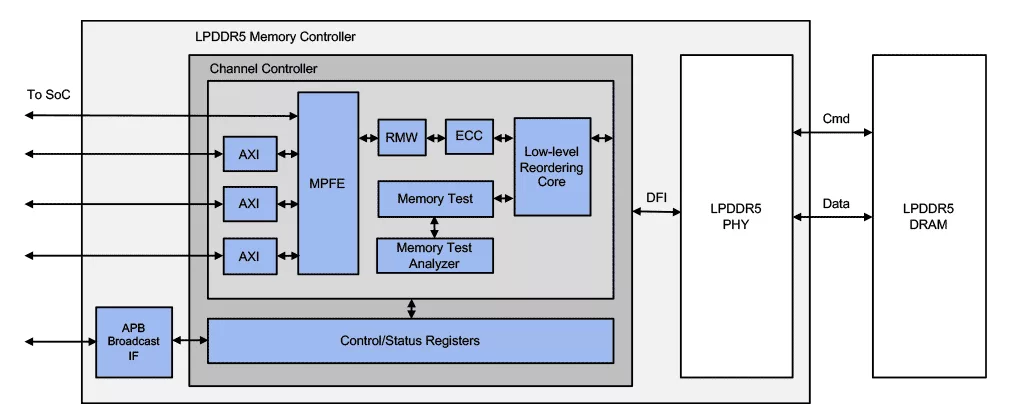
The LPDDR5 controller core accepts commands using a simple local interface and translates them to the command sequences required by LPDDR5 devices. The core also performs all initialization, refresh and power-down functions.
The core uses bank management logic to monitor the status of each LPDDR bank. Banks are only opened or closed when necessary, minimizing access delays.
The core queues up multiple commands in the command queue. This enables optimal bandwidth utilization for both short transfers to highly random address locations as well as longer transfers to contiguous address space. The command queue is also used to opportunistically perform look-ahead activates, precharges and auto-precharges further improving overall throughput.
Add-On Cores such as an AXI Core Bus Interface, Multi-Port Front-End and In-Line ECC Core can be optionally delivered with the core. The core can be delivered fully integrated and verified with the target LPDDR5 PHY.
Key features
- Support for all LPDDR5T/5X/5 devices
- Bank management logic monitors status of each bank
- Queue-based user interface with reordering scheduler
- Look-ahead activate, precharge, and auto-precharge logic
- Parity protection for all stored control registers
- PHY interface based on DFI 5.1 standard
- Each controller instance supports a single channel
- Multiple rank support (typically 2 or 4)
- Supports WCK:CK ratio 4:1
- Supports x16 mode
- Burst length BL16 and BL32
- Data bus inversion (DBI) feature (read and/or write)
- Supports masked write (MWR)
- Mode register write (MRW) and mode register read (MRR) functions
- Background ZQ calibration mode and command-based ZQ calibration mode
- Supports LPDDR5 speeds up to 9.6 Gbps/pin
- Supports all defined LPDDR5 channel densities (up to and including 32Gb, including non-binary densities)
- LPDDR5 bank architecture BG mode and 16B mode
- LPDDR5 per-bank refresh and all-bank refresh
- LPDDR5 refresh management
- LPDDR5 device self-refresh mode
- LPDDR5 device power-down mode
- Automatic generation of initialization and refresh sequences
- Built-in activity monitor
- Optional multi-burst capability
- Full set of add-on cores available
- Can be delivered fully integrated and verified with target LPDDR PHY
- Customization and integration services available
Block Diagram
Applications
- Mobile, Automotive, IoT, Laptop PCs, Edge
What’s Included?
- Core (source code)
- Testbench (source code)
- Complete documentation
- Maintenance updates
Files
Note: some files may require an NDA depending on provider policy.
Specifications
Identity
Provider
Learn more about LPDDR IP core
Cryptography Does Not Equal Security
The Growing Importance of AI Inference and the Implications for Memory Technology
DEEPX, Rambus, and Samsung Foundry Collaborate to Enable Efficient Edge Inferencing Applications
LPDDR6: The Next-Generation LPDDR Device Standard and How It Differs from LPDDR5
LPDDR flash: A memory optimized for automotive systems
Frequently asked questions about LPDDR IP
What is LPDDR5T / LPDDR5X / LPDDR5 Controller?
LPDDR5T / LPDDR5X / LPDDR5 Controller is a LPDDR IP core from Rambus, Inc. listed on Semi IP Hub.
How should engineers evaluate this LPDDR?
Engineers should review the overview, key features, supported foundries and nodes, maturity, deliverables, and provider information before shortlisting this LPDDR IP.
Can this semiconductor IP be compared with similar products?
Yes. Buyers can compare this product with similar semiconductor IP cores or IP families based on category, provider, process options, and structured technical specifications.