How Secure DDR Interfaces Protect DRAM from Memory Attacks
Brett Murdock, Dana Neustadter (Synopsys)
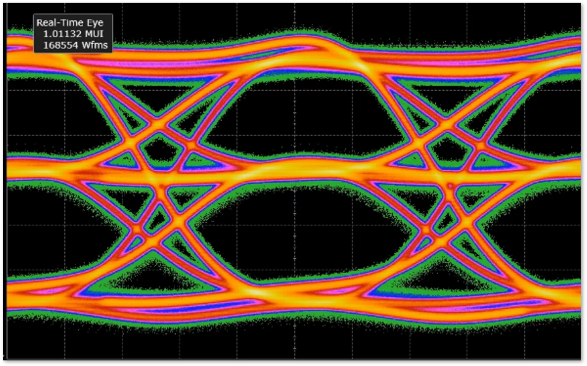
The GDDR7 PHY is fully compliant with the JEDEC GDDR7 standard, supporting data rates of up to 32 Gbps in PAM3 mode.
The GDDR7 PHY is fully compliant with the JEDEC GDDR7 standard, supporting data rates of up to 32 Gbps in PAM3 mode. In PAM3 mode, each byte consists of ten DQ signals and one DQE signal, while the GDDR7 also supports NRZ I/O signaling for low-power operation. With a maximum speed of 32 Gbps per pin, The GDDR7 PHY delivers a peak bandwidth of up to 128 GB/s per memory device. Designed for advanced FinFET process nodes, this PHY is optimized for seamless integration into cutting-edge applications.
The comprehensive product portfolio also includes full GDS delivery, signal integrity and power integrity (SI/PI) analysis, verification models, prototyping support, and simulation tools. These offerings empower customers to accelerate development cycles, ensure robust performance, and stay ahead in the competitive landscape of high-performance memory solutions.
Note: some files may require an NDA depending on provider policy.

GDDR7 PHY & Controller is a DDR IP core from Innosilicon Technology Ltd listed on Semi IP Hub.
Engineers should review the overview, key features, supported foundries and nodes, maturity, deliverables, and provider information before shortlisting this DDR IP.
Yes. Buyers can compare this product with similar semiconductor IP cores or IP families based on category, provider, process options, and structured technical specifications.