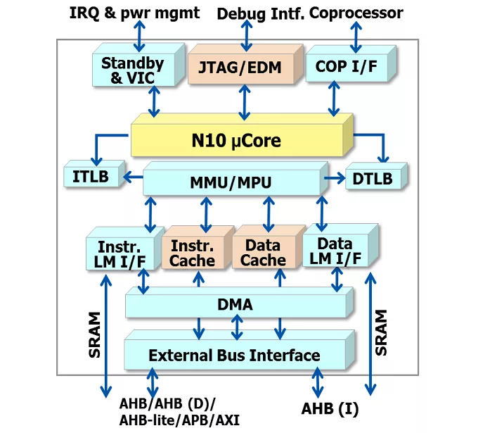
Overview
The mid-range Andes Technology N10 processor is ideal for applications ranging from consumer media players and smart glasses all the way to touch panel processing, motor control, and power management. The N10 features a 5-stage pipeline and operates at over 800 MHz clock rate providing plenty of performance for automotive electronics and industrial control. It also comes with I/D cache or local memory options that enable the core to more efficiently perform for networking or communication applications.
In the fast growing IoT market, the highly performance efficient N10 processor can be used as IoT gateway to bridge those ZigBee, Bluetooth or WiFi sensor devices to the internet connectivity. In addition, with the tightly-coupled IEEE-754 compliant NCESFP100 single-precision floating point unit (FPU), the N10 processor can be used in the high precision sensor devices to manipulate the data from ADC which converts physical continuous sensor signals to digital data.
Learn more about CPU IP core
For the first time in our more than 35-year history, Arm is delivering its own silicon products – extending the Arm Neoverse platform beyond IP and Arm Compute Subsystems (CSS) to give customers greater choice in how they deploy Arm compute – from building custom silicon to integrating platform-level solutions or deploying Arm-designed processors.
The ChiPy DSL is Quadric's Python framework for building complete on-chip pipelines. Using YOLOX-M as a case study, we show how backbone inference, box decoding, and NMS run entirely on the Chimera GPNPU — no host CPU intervention, no DDR round-trips, just Python compiled to silicon.
As part of the new Arm Lumex compute subsystem (CSS) platform, the Arm C1 CPU cluster – the first built on the Armv9.3 architecture – is the next evolution of our highest performing CPU cluster for consumer devices, designed to unleash the full potential of on-device AI and elevate the user experience.
Hardware fuzzing has recently gained momentum with many discovered bugs in open-source RISC-V CPU designs. Comparing the effectiveness of different hardware fuzzers, however, remains a challenge: each fuzzer optimizes for a different metric and is demonstrated on different CPU designs.
Unlock ultra-efficient performance, advanced AI processing, and robust security with the Cortex-A320—designed to power the future of IoT and edge AI innovation.
Pie maintains low computation latency, high throughput, and high elasticity. Our experimental evaluation demonstrates that Pie achieves optimal swapping policy during cache warmup and effectively balances increased memory capacity with negligible impact on computation. With its extended capacity, Pie outperforms vLLM by up to 1.9X in throughput and 2X in latency. Additionally, Pie can reduce GPU memory usage by up to 1.67X while maintaining the same performance. Compared to FlexGen, an offline profiling-based swapping solution, Pie achieves magnitudes lower latency and 9.4X higher throughput.