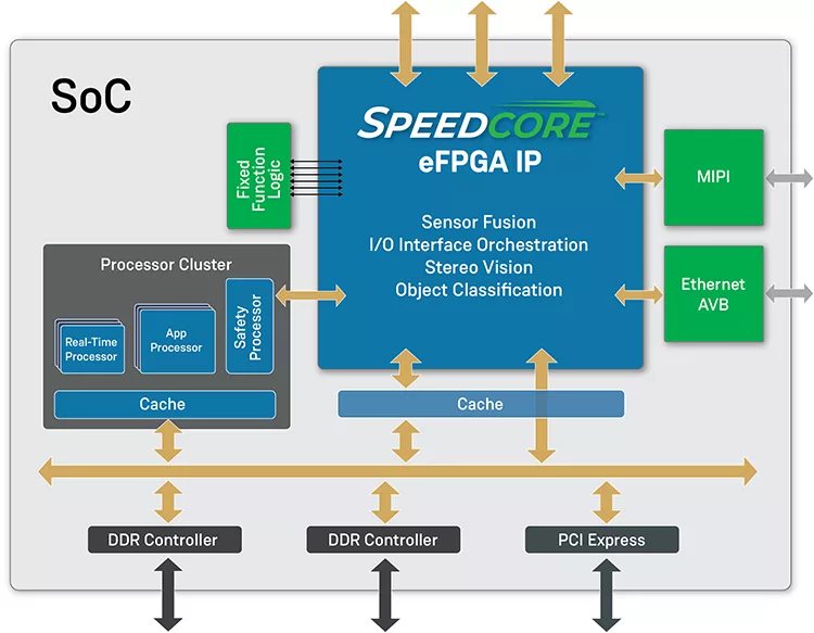
Speedcore embedded FPGA (eFPGA) IP has brought the performance and flexibility of programmable logic to ASICs and SoCs. Customers can integrate a Speedcore eFPGA IP into an ASIC or SoC for high-performance, compute-intensive and real-time processing applications such as artificial intelligence (AI), machine learning (ML), 5G wireless, networking, storage and automotive.
Speedcore eFPGA IP architecture incorporates many architectural enhancements that dramatically increase performance, reduce power consumption, and shrink die area. When selecting a Speedcore eFPGA, designers can select the optimal mix of architectural elements including:
- Logic – 6-input look-up-tables (LUTs) plus integrated wide MUX functions and fast adders
- Logic RAM – 2 kb per memory block for LRAM2k, and 4kb per memory block for LRAM4k
- Block RAM – 72 kb per memory block for BRAM72k, and 20kb per memory block for BRAM20k
- DSP64 – 18 × 27 multiplier, 64-bit accumulator and 27-bit pre-adder per block
- Machine learning processors (MLP) – 32 multiplier/accumulators (MACs) per block, supporting integer and floating point formats
Reconfigurable Logic Blocks (RLB)
- Logic – 6-input look-up-tables (LUTs) that implement all functions with as many as 7-inputs and some 8-input functions in a single level of logic. Reducing the need for multiple logic levels improves performance.
- 8:1 Muxes – New, dedicated 8-to-1 multiplexers dramatically increase logic performance.
- Shift chain – Double the number of registers compared to the original Speedcore architecture plus optimized routing for shift chains.
- ALU – A larger ALU now supports 8-bit operations for addition, counting, comparison, and maximum functions.
- LUT-based multiplication – Efficient, LUT-based multipliers require half the on-chip resources compared to other leading FPGA products: A 6 × 6 multiply requires only 11 LUTs and runs at 1 GHz. An 8 × 8 multiply requires only 18 LUTs and runs at 500 MHz.
Logic RAM
- The LRAM2k implements a 2,304-bit memory block configured as a 32 × 72 simple dual-port (one write port, one read port) RAM. The LRAM2k has a synchronous write port. The read port is configured for asynchronous read operations with an optional output register.
- The LRAM4k implements a 4,096-bit memory block configured as a 128 × 32 simple dual-port (one write port, one read port) RAM. The LRAM4k has a synchronous write port. The read port is configured for asynchronous read operations with an optional output register.
Block RAM
- The BRAM72k primitive implements a 72-kb simple-dual-port (SDP) memory block with one write port and one read port. Each port can be independently configured with respect to size and function, and can use independent read and write clocks. The BRAM72k can be configured as a simple dual port or ROM memory.
- The BRAM20k implements a dual-ported memory block where each port can be independently configured with respect to size and function. The BRAM20k can be configured as a single-port (one read/write port), dual-port (two read/write ports with independent clocks), or ROM memory.
DSP64
- The DSP64 blocks include multiple/accumulate and associated logic to efficiently implement math functions such as finite impulse response (FIR) filters, fast Fourier transforms (FFT), and infinite impulse response (IIR) filters. The DSP64 blocks are optimized to operate with the logic fabric and LRAM blocks to implement math functions.
Machine Learning Processor (MLP)
The new MLP in Speedcore eFPGA IP is a complete AI/ML compute engine. Each MLP includes a cyclical register file that leverages temporal locality to reuse stored/cached weights or data, thus boosting performance by significantly reducing data movement for a variety of calculations. The MLPs are tightly coupled with their neighboring MLPs and larger memory blocks to maximize processing performance and to deliver the highest number of operations per second with the lowest power profile. The MLPs support fixed-point and floating-point formats (Bfloat16; 16-bit, half-precision; and block floating point). Users can trade off precision versus performance by selecting the optimal data precision on the fly, as required by each application.
| Feature |
Benefit |
| Configurable multiply precision and count |
Trade off performance/power vs. precision - Increasing multiplier count for lower precision functions. |
| Cyclical register file |
Double compute performance - Similar to a cache function in that data is saved for efficient reuse by the MLP. Optimized for AI/ML functions. |
| Column bonding and MLP cascade paths |
Higher performance - Hard paths between memory and other MLP blocks enable high-performance functionality while freeing up general-purpose routing.
|
| Multiple number formats |
Flexibility - Supports mainstreams fixed- and floating-point formats and frameworks. |
| Rounding and saturation |
System performance - Support for multiple rounding formats and saturation that would otherwise need to be implemented in LUTs. |
Routing
- Dedicated buses – A first in the eFPGA industry! High-performance, bus-grouped routing channels, separate from the standard eFPGA routing channels, ensure that there is no congestion between bus-oriented data traffic — common with memories — and other types of data traffic routed over the eFPGA’s standard, bit-oriented channels.
- Bus muxes – Another first in the eFPGA industry; bus muxes allow users to efficiently create bus mux functions without consuming any LUTs or standard routing. This capability effectively creates a giant, distributed, run-time-configurable switching network that is separate from the eFPGA’s bit-oriented routing network.
Integrating Speedcore eFPGA IP
While the Speedcore design and integration methodology is highly flexible and can accommodate significant variations in SoC/ASIC development flows, there are some general principles and guidelines which, if followed, will make the development and integration effort simpler, smoother and more efficient:
- The Speedcore eFPGA requirements must be defined early in the ASIC development process, including the mix of Speedcore programmable logic blocks needed for the target design(s), the physical dimensions of the desired Speedcore eFPGA and the metal stack of the target process technology. Defining these aspects early will streamline the Speedcore integration effort, as it will allow for ASIC design details such as the interface between hardwired ASIC circuitry and the Speedcore I/O boundary, routing in the metal stack, power management and ASIC circuit block layout to be worked out quickly and efficiently.
- ASIC designs typically operate above 1 GHz, whereas FPGA designs typically operate between 300 MHz and 500 MHz. As a result, the functionality in the Speedcore eFPGA will typically need to operate on separate clock domains and require interface circuitry for crossing clock domain. It is important to define the interface between the host ASIC and the Speedcore instance early on and verify that the implementation meets performance both in the ASIC and Speedcore instance with real or example designs that will target the Speedcore instance once the ASIC is completed.
With the above in mind, a quick summary of the design and integration methodology is as follows:
- Run benchmarks: The most important decision for a Speedcore implementation is determining how many programmable resources (LUTs, embedded memories, DSP blocks, etc.) are needed for the application. The best methodology to determine the optimal resource count is to run benchmarks through the Achronix CAD Environment (ACE) design tools using typical designs that will later be hosted in the final Speedcore instance. These designs should include any interface functions required to transfer data between the host ASIC and the Speedcore instance.
- Sizing the Speedcore instance: Based on the benchmark results, the process technology and metal stack of the host ASIC, Achronix can provide the resulting die size and aspect ratio for the Speedcore instance. Speedcore IP is a fully modular architecture which can be scaled from small implementations with less than 10,000 LUTs up to very large implementations with over 1 million LUTs. There is also great flexibility in determining the right aspect ratio.
- Finalize business terms: Achronix has a standard contract to license Speedcore IP and a specification template for the customer to define requirements for operating conditions, physical dimensions, resource counts, configuration modes and features, pin counts and interface details, clocks, size, performance, power, testing details and quality specifications. This contract forms a complete framework for defining a Speedcore implementation.
- Speedcore development: There are three phases of delivery from Achronix during the development of a Speedcore instance. The first phase includes preliminary physical pin information and timing. The next phase includes all deliverables for the Speedcore instance along with preliminary timing. The final delivery includes all deliverables for the Speedcore instance with final timing. A version of ACE is included with each delivery phase.
- DFT: Shortly after delivering the Speedcore IP, Achronix delivers DFT simulation and ATE vector files for testing. Achronix will then work alongside the customers or manufacturers ATE engineers to ensure that all ATE vectors are successfully ported across, and all tests pass, thus ensuring a smooth transition to a production flow.