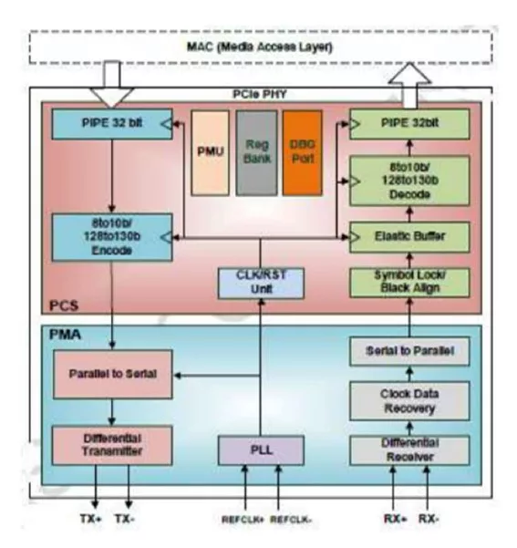
Overview
This PCIe 3.0 Base Specification-compliant Peripheral Component Interconnect Express Gen3 PHY supports the PIPE 4.3 interface standard. Due to the support of an extra PLL control, reference clock control, and inbuilt power gating control, low power consumption is accomplished. Additionally, because the low power mode option is customizable, the PHY is extensively useful for a variety of settings with diverse power consumption considerations. Utilizing a test bench created in Verilog HDL, NCVerilog simulation software is used to verify PCIe PHY operation.
Provider
T2M GmbH is the leading Global Technology Company supplying state of the art complex semiconductor connectivity IPs and KGDs, enabling the creation of complex connected devices for Mobile, IoT and Wearable markets.
T2M's unique SoC White Box IPs are the design database of mass production RF connectivity chips supporting standards including Wifi, BT, BLE, Zigbee, NFC, LTE, GSM, GNS. They are available in source code as well as KGD for SIP / modules.
With offices in USA, Europe, China, Taiwan, South Korea, Japan, Singapore and India, T2M’s highly experienced team provides local support, accelerating product development and Time 2 Market.
Learn more about Multi-Protocol PHY IP core
Morgan State University (MSU) recently received an Apple Innovation Grant, designed to support engineering schools as they develop their silicon and hardware technologies. The New Silicon Initiative (NSI) is designed to inspire and prepare students for careers in hardware engineering, computer architecture, and silicon chip design.
Increasingly, more of the focus on mobile has centered around cloud datacenters and the networking to get the data back and forth between these datacenters and the mobile device. Functions like voice recognition and mapping depend on the ability to split the functionality between the smartphone, for local processing like encryption and compression, and the back end, where a large number of servers can do the heavier lifting before returning the results.
Steven Brown
The Cadence 10G multi-protocol PHY was architected to address this exact challenge. Designed to scale across multiple process nodes, it consolidates PCI Express (PCIe), USB, DisplayPort, Ethernet, and other interfaces into a single, compact, silicon-efficient block. What sets it apart is simultaneous multi-protocol support, which enables multiple data paths without duplicating hardware, requiring extra board connectors, or paying the area and power penalty of separate IP blocks.