Vendor: TES Electronic Solutions Category: GPU

3D OpenGL ES 1.1 GPU IP core

D/AVE 3D is cost-efficient IP core for 3D graphics applications.

Overview

D/AVE 3D is cost-efficient IP core for 3D graphics applications. This core is available for FPGAs, ASICs and SOCs, specifically designed for the embedded, automotive and infotainment market with a big emphasis on flexibility both in hardware and the software.
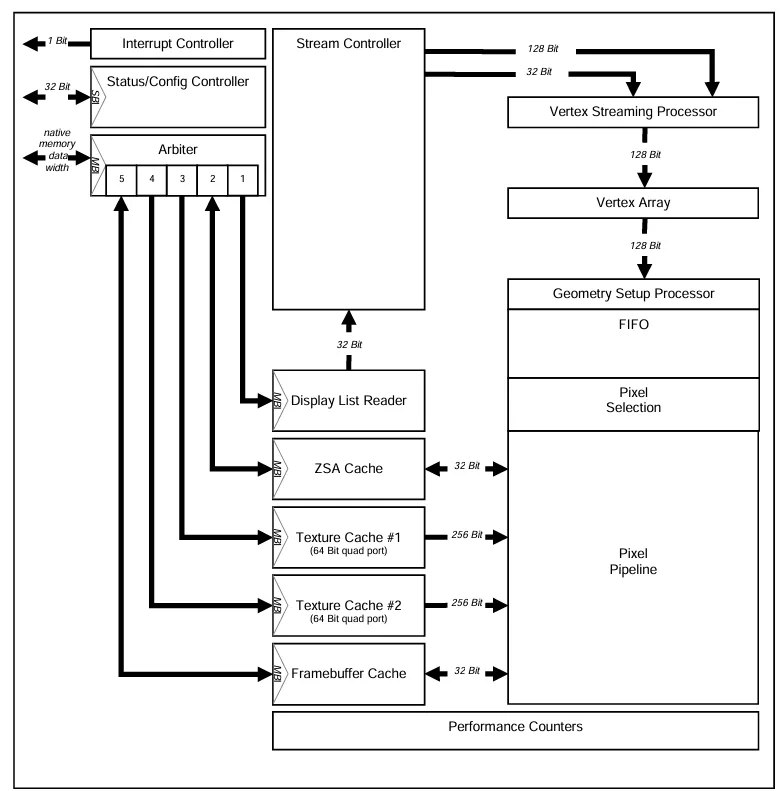
Architecture


The system interfaces to D/AVE 3D are very simple. In the Altera world it supports all bus interfaces available on Avalon bus architecture. In the SOC world AMBA is supported and additional bus wrappers are easy to implement with the interfaces to D/AVE 3D being very simple Master, Slave and Interrupt lines. After reset the CPU can configure or can get status information via the SBI (Slave Bus Interface) with data and memory access through the master bus interface.

To deal with unpredictable memory latency, FIFOs are added at all crucial places, which makes D/AVE 3D more performance robust. The pixel pipeline supports early Z-test. D/AVE 3D in a SOC supports multiple pixel pipelines.

Performance

All performance data given are made under the following assumptions:

  • 100% cache hit rates
  • No latency from external data
  • Internal pipeline latency ignored
  • 100 MHz.

Fillrate

The Pixel-Pipeline of the D/AVE 3D-IP can produce 1 pixel per cycle, in any configuration.

Vertex Throughput

The vertex throughput depends very much on how many light sources are enabled and if transformation is performed. It also depends on the associated vertex attributes, such as color and texture coordinates.

Transformation Lighting Shade Model Texture Coordinates Performance
(Vertices Per Second)
- - Flat - 33 Mio.
4x4 Matrix - Flat - 6,6 Mio
4x4 Matrix - Smooth - 6,25 Mio.
4x4 Matrix - Smooth S, T 5,8 Mio
4x4 Matrix 1xDiffuse
1xAmbient
Smooth - 0,3 Mio.

Triangle Throughput

The triangle throughput depends very much on the number of attributes, which have to be interpolated across the primitive.

Z-Buffer Vertex Colors Texure Coordinates Performance (Triangles Per Second)
  - - 6,6 Mio.
x x - 5,2 Mio.
x - S1, T1 6,6 Mio.
x x S1, T1 4 Mio.
x x S1, T1/ S2, T2 3,5 Mio.


Key features

  • Low resource usage
    • Low gate count ( ~1Mio. Gates for ASIC)
    • Low internal memory requirements ( ~125 K Memory Bits)
    • 70K Logic elements for FPGAs
  • Offers a wide range of graphical primitives
    • Lines, Triangles, Quadrangles
  • Prepared for easy SoC integration
    • ALTERA AVALON support
    • ARM AMBA-AHP, ARM AMBA-APB Bus support
    • Performance robust to high memory latency
    • Single clock domain architecture
  • High Performance
    • 100 Mio. Pixels/Second fill rate (100 MHz).
    •  6,6 Mio. triangles throughput (100 MHz.)
    • Early-Z-Test
  • High Quality Rendering
    • Anti-Aliasing and Sub-Pixel accurate rendering
    • Edge-Based-Filtering for image scaling
    • Per-Primitive-Anti-Aliasing (settable per edge)
    • Static dithering at Framebuffer write back to enhance RGB565 output
  • Fully programmable Transform and Lighting Engine
  • Textures
    • 2048 x 2048 Texture size
    • Flexible texture color format handling
    • Texture compression
    • Texture offset swizzeling
  • Framebuffer
    • 2048 x 2048 supported
    • ARGB8888, ARGB4444, ARGB1555, RGBA5551, RGB565, AL88, AL44, A8
    • Blend Modes - Blend, Multiply, Darken, Lighten

Block Diagram

What’s Included?

APIs

D/AVE 3D is provided with the following APIs. The drivers are reentrant and OS agnostic.

  • EGL 1.3 API
  • OpenGL ES 1.1 API
  • OpenVG 1.01 API

Files

Note: some files may require an NDA depending on provider policy.

Specifications

Identity

Part Number
D/AVE 3D
Vendor
TES Electronic Solutions

Provider

TES Electronic Solutions
HQ: Germany
TES Electronic Solutions is a global electronic technology and services company offering innovative solutions and custom electronic design as well as a blend of hardware (for ASICs and FPGAs) and software IP. Besides designing customer specific systems or sub-systems that are optimized to customers’ applications, TES also develops licensable wireless, graphics,GUI, video-IO and multimedia IP accelerating time to market. From its design centers in Germany, and with its broad expertise in GUI concepts, industrial design, hardware-, software-, FPGA- and ASIC-development TES provides innovative solutions in the areas of RF / wireless, professional multimedia, embedded graphics and RF / mixed-signal ASICs. TES serves a wide range of customers from well-known highly specialized middle-size companies to global market leaders.

Learn more about GPU IP core

Tape-out Risk in the Age of Edge AI: The Case for GPU IP

A full SoC tape-out at 5nm approaches $400M in fully loaded, non-recurring engineering and mask costs. At 3nm, estimates push past $600M. Every IP block on that die is a commitment to a set of assumptions about what the silicon will need to do. In AI, those assumptions have a shorter shelf life than they used to.

What Does a GPU Have to Do With Automotive Security?

The automotive industry is undergoing the most significant transformation since the advent of electronics in cars. Vehicles are becoming software-defined, connected, AI-driven, and continuously updated. This evolution brings extraordinary new capability – but it also brings greater levels of cybersecurity and functional-safety risks.

How Alternate Geometry Processing Enables Better Multi-Core GPU Scaling

Scaling GPU performance across multiple cores sounds simple in theory: add more cores, get more performance. In practice, it’s one of the toughest challenges in graphics architecture. While some workloads scale well thanks to their independent nature, some workloads, especially geometry processing, introduce order dependencies that make linear performance scaling a tricky problem to solve for every GPU architecture in the industry.

NVIDIA GPU Confidential Computing Demystified

In this paper, the authors aim to demystify the implementation of NVIDIA GPU-CC system by piecing together the fragmented and incomplete information disclosed from various sources.

Frequently asked questions about GPU IP cores

What is 3D OpenGL ES 1.1 GPU IP core?

3D OpenGL ES 1.1 GPU IP core is a GPU IP core from TES Electronic Solutions listed on Semi IP Hub.

How should engineers evaluate this GPU?

Engineers should review the overview, key features, supported foundries and nodes, maturity, deliverables, and provider information before shortlisting this GPU IP.

Can this semiconductor IP be compared with similar products?

Yes. Buyers can compare this product with similar semiconductor IP cores or IP families based on category, provider, process options, and structured technical specifications.

×
Semiconductor IP