Intel, TSMC to detail 2nm processes at IEDM
By Peter Clarke, eeNews Europe (October 8, 2024)
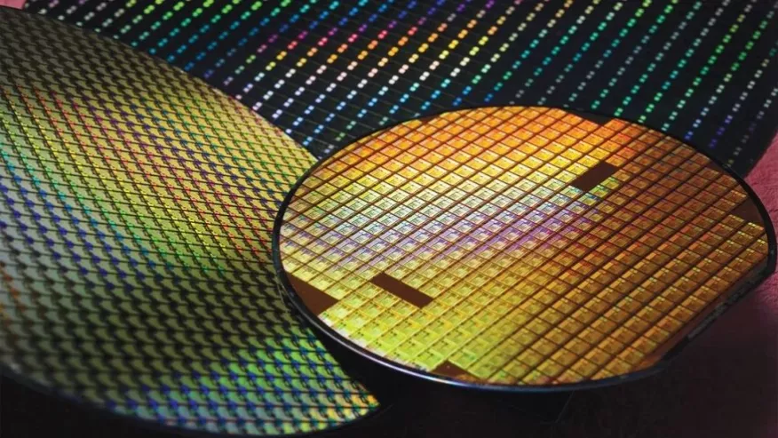
Intel’s attempts to get back to the leading-edge in chipmaking and foundry TSMC’s steps defining that leading-edge will be on show at this year’s International Electron Devices Meeting (IEDM) coming up in December, in San Francisco.
In a late news paper, researchers from TSMC will unveil the N2 manufacturing process, which is a nominal 2nm process designed for computing in AI, mobile and high-performance computing. In the following paper in the same session Intel engineers will provide details of scaling RibbonFETs, the name Intel gives to its nanosheet transistors.
To read the full article, click here
Related Semiconductor IP
- UCIe D2D Adapter & PHY Integrated IP
- Low Dropout (LDO) Regulator
- 16-Bit xSPI PSRAM PHY
- ASIL B Compliant MIPI CSI-2 CSE2 Security Module
- SHA-256 Secure Hash Algorithm IP Core
Related News
- Analog Bits to Demonstrate IP Portfolio on TSMC 3nm and 2nm Processes at TSMC 2025 Technology Symposium
- Alphawave Semi Tapes Out Breakthrough 36G UCIe™ IP on TSMC 2nm, Unlocking Foundational AI Platform IP on Nanosheet Processes
- Intel and Cadence Expand Partnership to Enable Best-in-Class SoC Design on Intel's Advanced Processes
- Siemens qualifies industry-leading IC design solutions for Intel Foundry processes
Latest News
- Alchip Appoints Freddy Engineer Chief Business Officer and North America General Manager
- Perceptia Devices and Dolphin Semiconductor Partner to Deliver Best-in-Class IP Portfolio Covering Power Management, Clocking, High-Quality Audio and In-Situ Monitoring
- TSMC Chases Soaring AI Demand
- EU DARE Project Is Scrambling to Replace Codasip
- Sofics and Alcyon Photonics Partner to Support Next-Generation Photonic Systems