针对需满足DO-254 标准规范的PCIe航空电子设计,业界首次使用事务级建模 (TLM) 实现全速验证
Aldec helps Thales evaluate the use of transaction level modeling for FPGA designs that use high-speed bus interfaces, apply high-level test scenarios, verify 100% FPGA-level requirements by test and shorten the company’s overall verification times.
Henderson, NV, USA – January 12, 2022 – Aldec, Inc., a pioneer in mixed HDL language simulation and hardware-assisted verification for FPGA and ASIC designs, has helped Thales evaluate the use of transaction-level modeling (TLM) for the verification of a PCIe-based FPGA design requiring DO-254 compliance. This is believed to be the first use of TLM in avionics with design assurance level (DAL) A or B classification.
FPGA designs that use asynchronous clocks with multiple high-speed serial interfaces such as PCIe produce non-deterministic results during physical tests. Simulation results are optimized because they are based on simplified models, while the test results in physical hardware depend on the phases of clock oscillators. Bit-level verification struggles with this, especially when comparing in-hardware results against simulation results, and many false errors are likely to be observed. For these reasons, Thales decided to work with Aldec to explore a new verification approach based on TLM.
“Before we trialed TLM, the problem we had was that we had a model of what the PCIe interface does, but it was not cycle accurate,” comments Yann, FPGA designer and a member of Thales’ verification team. “This introduced timing differences in the overall design under test’s [DUT’s] reaction to the bit-level PCIe transactions. We could not certify to DO-254 with such discrepancies.”
“TLM is a popular design/verification methodology from the semiconductor industry, and it works at a higher level of abstraction than bit-level,” explains Louie De Luna, Director of Marketing at Aldec. “With TLM the design interfaces are abstracted and there is no need to deal with bit-level details during verification. Transactions are easier to manage and correlate with the simulation results, therefore traceability is much easier to establish. Also, the untimed testbenches used with TLM are not sensitive to clock frequency and phase changes, which is ideal for verifying SoC FPGA designs with non-deterministic behavior.”
The verification platform used for the research project was Aldec’s DO-254/ED-80 compliance tool set (CTS), a hardware/software solution Thales has been using since 2008 for the bit-level verification of their FPGA designs.
The CTS features a fit-for-purpose daughter board that mimics the target FPGA design based on multiple asynchronous clocks, I/Os, high-speed interfaces and, most importantly, the FPGA device that will be used in the end product. In addition, the testbench used for simulation (i.e. simulated operating scenarios) is reused for at-speed, in-hardware verification.
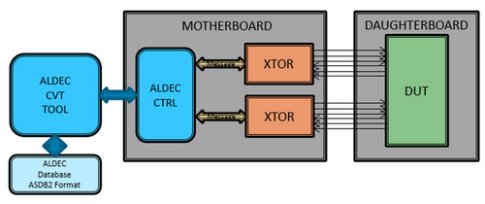
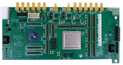
For the research project, Aldec designed and supplied a custom daughterboard with the target FPGA (with PCIe) plus synthesized PCIe transactors (XTORs) for inclusion on the motherboard and which allows transactions captured during simulation to be applied to the physical DUT in real time.
“Throughout the whole process, we defined with Aldec the kind of features we needed within the software of their CTS, and they reacted quickly,” continues Yann. “Aldec also helped us run a variety of test scenarios to make sure our flow was robust enough to be used on a number of different real projects.”
The project has produced extremely encouraging results and Thales is currently evaluating its new verification flow internally on a real project. The flow will then be presented to the certification authorities.
“We have a long-standing relationship with Thales, ever since they adopted our CTS in 2008,” concludes De Luna. “Thales was able to achieve compliance approval across multiple programs with the CTS as the main FPGA physical test system for verifying 100% FPGA-level requirements by test, at the bit-level. It’s truly an honour for us to remain a trusted partner and a reliable solution provider as Thales introduces high-speed bus interfaces into their FPGA designs.”

Above, transactors interface with the design under test replicate real-life behavior and to avoid timing-related false errors where high-bus interfaces (like PCIe) are concerned.

Above, the custom daughterboard (including target FPGA with PCIe) Aldec made for Thales’ proof-of-concept project.
Related Semiconductor IP
- ARINC 664 (AFDX) End System DO-254 IP Core
- DO-254 compliant MIL-STD-1553B IP core
- 10/100/1000 Ethernet MAC DO-254 IP Core
- CAN Controller DO-254 IP Core
- CAN FD Controller DO-254 IP Core
Related News
- Synopsys的SpyGlass解决方案提供关键技术以符合DO-254航空安全标准
- SmartDV与Aldec强强联手,将SmartDV的验证IP与Aldec的Riviera-PRO 仿真器 紧密相连
- 来自CAST 的HDLC / SDLC IP内核现可支持机载系统 DO-254规格要求
- Avery Design推出PCI Express 6.0验证IP实现早期开发、标准合规性评审检查