Vendor: Key ASIC Category: Single-Protocol PHY

USB2.0 PHY, 8-bit or a 16-bit parallel interface, remaining backward compatible with USB1.1 legacy protocol at 12Mbps

KA13UGUSB20ST001 is USB2.0 physical layer transceiver (PHY) integrated circuits.

Overview

KA13UGUSB20ST001 is USB2.0 physical layer transceiver (PHY) integrated circuits. The PHY can be configured for either an 8-bit or a 16-bit parallel interface, which complies with the USB Transceiver Macrocell Interface (UTMI) specification. It supports 480bps transfer rate, while remaining backward compatible with USB1.1 legacy protocol at 12Mbps.

It includes the following blocks:
* Analog Driver and Receiver
* PLL generate the 480MHz clock
* Clock and Data Recovery
* NRZI encoder/decoder
* Serialize / De-serialize
* Control state machine
* Integrated pull up and self-calibrated termination resistors and switches

Key features

  • Complies with Universal Serial Bus Specification Rev. 2.0
  • Interface compliant with the UTMI specification (60MHz 8-bit interface or 30MHz 16-bit interface)
  • Supports 480Mbps High-Speed(HS) and 12Mbps Full-Speed(FS)
  • Serial data transmission rates
  • Built-In Self Test (BIST)
  • Integrated Self-Calibrated termination resistors (45 ohm) and built-in 1.5K ohm
  • Power supply: VDD33=3.3V ±10%, VP12=1.2V ±10%
  • Operating temperature: -40°C~ +125°C

Block Diagram

Benefits

  • Physical layer transceiver (PHY), 8-bit or a 16-bit parallel interface, remaining backward compatible with USB1.1 legacy protocol at 12Mbps
  • Supports 480bps transfer rate, while remaining backward compatible with USB1.1 legacy protocol at 12Mbps.

Applications

  • Digital Video camera
  • Scanner
  • Printer
  • External storage devices, e.g.Portable hard disk, Optical drive (CD-ROM, CD-RW, DVD)

What’s Included?

  • Data Sheet
  • Integration guide
  • LEF
  • Timing LIB
  • Verilog PHY behavioral model and BIST test-benches
  • EVB schematic and user guide

Specifications

Identity

Part Number
KA13UGUSB20ST001
Vendor
Key ASIC
Type
Silicon IP

Provider

Key ASIC
HQ: Malaysia
Key ASIC was incorporated in the year 2005. In 2006, we were awarded Multimedia Super Corridor (MSC) Status by the Malaysia Digital Economy Corporation (MDEC). We started with the design of IP, ASIC, and SoC. In 2009, we were listed on the main board of KLSE. Khazanah and CIMB are our main investors. Key ASIC is not only a leading ASIC / SoC design service company, we are also a turnkey service company from spec-in to system module that focuses on AI chips, IoT, and medical applications. We are committed to providing customers with competitive SoC professional one-stop design services in terms of PPA (Performance, Power, and Area). Based in Kuala Lumpur, Malaysia with R&D Centers in Malaysia and Tai Yuen Hi-Tech Industrial Park Taiwan, Key ASIC provides ODM and OEM of ASIC design services from Specification, RTL, Netlist to silicon, as well as process migration from GDSII. Our experienced SoC designer and engineers combined with extensive manufacturing, logistics resources, and a flexible engagement model can provide Key ASIC customers with a comprehensive support system for modular ASIC innovation from IP development through prototype to production.

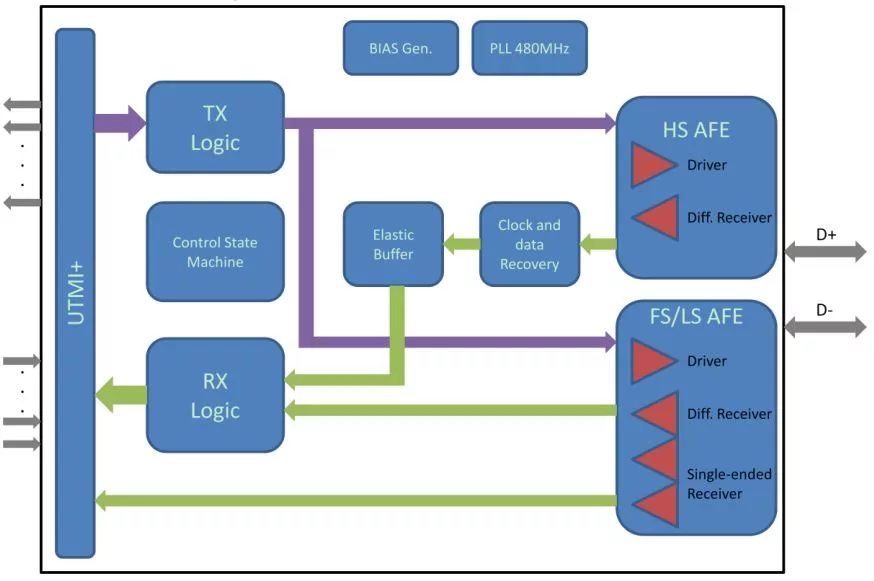
Learn more about Single-Protocol PHY IP core

UFS Goes Mainstream

UniversalFlash Storage (UFS) was created for mobile applications and computer systems requiring high performance and low power consumption. These systems typically use embedded Flash based on the JEDEC standard eMMC. UFS was defined by JEDEC as the evolutionary replacement for eMMC offering significantly higher memory bandwidth. The standard builds on existing standards such as the SCSI command set, the MIPI Alliance M-PHY and UniPro as well as eMMC form factors to simplify adoption and development.

Design IP Faster: Introducing the C~ High-Level Language

In this paper, we introduce a new high-level, dataflow programming language called C~ (“C flow”) that further increases productivity by raising the level of abstraction from behavioral descriptions, while overcoming the limitations of C for hardware design. We present the syntax and semantics of this language, and the framework that provides hardware and software code generation. This paper illustrates the benefits of using C~ for hardware design of a IEEE 802.3 MAC, synthesized for FPGA and for 90nm CMOS technology.

Universal Flash Storage: Mobilize Your Data

Universal Flash Storage (UFS) was created for mobile applications and computer systems requiring high performance and low power consumption. These systems typically use embedded Flash based on the JEDEC standard eMMC. UFS was defined by JEDEC as the evolutionary replacement for eMMC offering significantly higher memory bandwidth. The standard builds on existing standards such as the SCSI command set, the MIPI Alliance M-PHY and UniProSM as well as eMMC form factors to simplify adoption and development.

Can MIPI and MDDI Co-Exist?

Since MIPI and MDDI standards both target interfaces to cameras and displays on mobile devices, are two separate standards really needed?

Frequently asked questions about Single-Protocol PHY IP

What is USB2.0 PHY, 8-bit or a 16-bit parallel interface, remaining backward compatible with USB1.1 legacy protocol at 12Mbps?

USB2.0 PHY, 8-bit or a 16-bit parallel interface, remaining backward compatible with USB1.1 legacy protocol at 12Mbps is a Single-Protocol PHY IP core from Key ASIC listed on Semi IP Hub.

How should engineers evaluate this Single-Protocol PHY?

Engineers should review the overview, key features, supported foundries and nodes, maturity, deliverables, and provider information before shortlisting this Single-Protocol PHY IP.

Can this semiconductor IP be compared with similar products?

Yes. Buyers can compare this product with similar semiconductor IP cores or IP families based on category, provider, process options, and structured technical specifications.

×
Semiconductor IP