Vendor: ASICS World Services, LTD. Category: SATA Controller

Serial ATA I/II Device Controller IP Core

The Serial ATA Device Controller IP Core provides an interface to high-speed serial link replacements for the parallel ATA attach…

Overview

The Serial ATA Device Controller IP Core provides an interface to high-speed serial link replacements for the parallel ATA attachment of mass storage devices. The serial link employed is a high-speed differential layer that utilizes Gigabit technology and 8b/10b encoding.

This core is fully compliant to the Serial ATA 1.0a specification and provides some features of the Serial ATA II extensions.
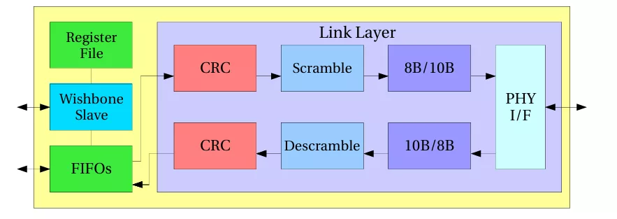
ARCHITECTURE

The Serial ATA Link and Transport Layer Core implements a serial ATA device interface which connects to a SATA PHY via a 10bit interface and provides a WISHBONE slave interface for register and DMA access. It consists of the link layer module- with 10bit data paths to the physical layer- and a transport layer module which connects to the system via a WISHBONE slave interface.

SAPIS PHY INTERFACE

This interface connects to any SAPIS compliant serial ATA PHY. Power management and speed negotiation signals are included. The PHY interface is synchronous to the PHY clock domain, which may have a different clock frequency than the system clock domain. Synchronization is done by the Serial ATA Link and Transport Layer Core.

WISHBONE SLAVE INTERFACE

The slave interface is used to access all core internal registers as well as the data FIFO.

SIZE AND SPEED

Software or an external DMA unit can write transmit data into the data FIFO or can read from the FIFO.

DMA HANDSHAKE

Simple handshake signals are provided to connect a DMA unit to the core module. The DMA requests will be asserted as soon as any transmit data is available or is needed in the core's data FIFO. The DMA unit will then access the data FIFO via the WISHBONE slaveinterface. A system interrupt will inform device software on completion of a data transfer.

Automatic flow control mechanisms control data throttling to avoid underflow or overflow of the transmit data FIFO. The DMA unit (or device software) may work at any speed without the risk of data loss. Data FIFO thresholds can be adjusted to optimize the data flow control.

Key features

  • 10 bit Phy interface 
  • Connects to SAPIS compliant serial ATA Phy
  •  Fully compliant to SATA Gen 1(1.2 Gb/s) and  Gen 2 (2.4 Gb/s)
  •  Wishbone slave interface for register access  and FIFO/DMA data transfers
  •  Only very few FF's in the Phy clock domain,  main part on the Wishbone clock
  •  128 byte (32 double word) data FIFO (optional  256 byte) 
  •  Parallel ATA legacy software compatibility 
  • Implements the Task File, the non-standard  serial ATA status and control registers,  specific device registers and native mode  registers
  •  interrupt and DMA handshake (external  DMA) 
  • 48-bit address feature set supported 
  • 8b/10b coding and decoding 
  • CONT and data scramblers to reduce EMI
  •  CRC generation and checking
  •  Auto inserted HOLD primitives
  •  Power management support (partial and  slumber)
  •  Optional native mode programming model
  •  Many configuration options

Block Diagram

Benefits

  • Flexible
  • Compact
  • Cost-effective

What’s Included?

  • Verilog Source Code
  • Test Bench
  • Sample Synthesis scripts
  • Documentation
  • Reference Design

Specifications

Identity

Part Number
SATA_DEVICE1
Vendor
ASICS World Services, LTD.
Type
Silicon IP

Files

Note: some files may require an NDA depending on provider policy.

Provider

ASICS World Services, LTD.
ASICs World Services specialize in providing top-notch IP Cores and design services. We will assist you in any phase of the design cycle, or take your idea from the conceptual stage to final product. With over 60 years of experience in the field, we have a long list of successfully completed projects.

Learn more about SATA Controller IP core

An Effective way to drastically reduce bug fixing time in SoC Verification

Many times we are not aware of very useful EDA tool options which are already available. Even if such options are very well documented, we don't look at them and try them. But some options are very useful and if you know them, it makes job of design engineer and/or verification engineer very easy. Here, I am going to talk about one very powerful and useful VSIM option of QuestaSim. It is VCDSTIM option of VSIM.

Designing Around an Encrypted Netlist: Is The Pain Worth the Gain?

Oftentimes, in order to save on the cost of IP, a company will select an encrypted netlist as the deliverable instead of the RTL source code. This is especially common among companies looking to develop in FPGA devices where they can often get the necessary IP from their FPGA vendor.

STBus complex interconnect design and verification for a HDTV SoC

To support High Definition Television (HDTV) application, the System on Chip (SoC) presented in this paper has to support multiple and concurrent internal processes. Most of these operations read data from memory, process them and store the resulting data into memory. Each functional unit of the system is responsible for a specific data processing, but all the data are stored in the same shared external memories.

Frequently asked questions about SATA Controller IP

What is Serial ATA I/II Device Controller IP Core?

Serial ATA I/II Device Controller IP Core is a SATA Controller IP core from ASICS World Services, LTD. listed on Semi IP Hub.

How should engineers evaluate this SATA Controller?

Engineers should review the overview, key features, supported foundries and nodes, maturity, deliverables, and provider information before shortlisting this SATA Controller IP.

Can this semiconductor IP be compared with similar products?

Yes. Buyers can compare this product with similar semiconductor IP cores or IP families based on category, provider, process options, and structured technical specifications.

×
Semiconductor IP