PCIe 7.0 Switch with with Time Division Multiplexing
The PCI Express® (PCIe®) 7.0 Switch is a customizable, multiport embedded switch for PCIe designed for ASIC and FPGA implementati…
Overview
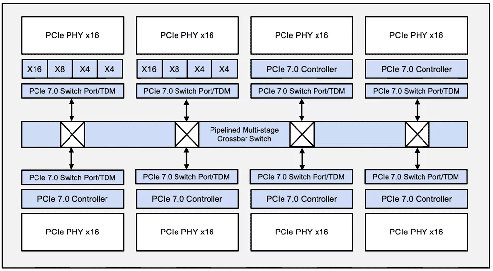
The Rambus PCI Express® (PCIe®) 7.0 Switch is a customizable, multiport embedded switch for PCIe with TDM support designed for ASIC and FPGA implementations. It enables the connection of one upstream port and multiple downstream ports as a fully configurable interface subsystem. It is backward compatible to PCIe 6.3 and PCIe 5.0.
How the PCIe 7.0 Switch Works
The PCIe 7.0 Switch is the first embedded PCIe 7.0 switch IP available on the market and enables designers to use fewer PCIe PHYs, saving latency, power consumption and bill-of-material costs. The PCIe switch IP transparently manages upstream-downstream data flow as well as peer-to-peer transfers between downstream ports, delivering the flexibility, scalability and configurability required for connecting multiple devices, including NVMe SSDs.
Key features
PCI Express Interfaces
- Up to 2 upstream port, up to 31 downstream ports
- Up to 128 lanes
- Bifurcated port groups – x16 down to x4 with TDM support
- Up to x16 link width per port
- Link rate of 2.5, 5, 8, 16, 32, 64 and 128 GT/s per lane
- Supports PCIe Base Revision 7.0 and 6.3
- Supports PHY Interface for PCIe (PIPE) 7.0
- Single Virtual Channel (VC) implementation
- Configurable PIPE interface (8-bit, 16-bit, 32-bit, 64-bit, 128 bit)
- Configurable Receive and Replay buffer sizes
- Advanced Error Reporting (AER) supported on each port
- ECRC generation and check
- ARI supported
- Lane reversal supported
- Independent configuration of link width, link speed, equalization settings, and PIPE interface width per-PCIe port
- Support for Hot Plug on every downstream port
Switching Logic
- PCIe TLP routing: Configuration, Memory Write/Read, I/O and Messages Packets
- L1 and wake-up events forwarding
- Peer-to-Peer transactions support between downstream ports
- Configurable Egress Buffer for non-blocking output queueing switch performance
- Broadcast and Multicast supported
- Downstream Port Containment (DPC) supported
- Round-Robin arbitration
- Built-in advanced data protection including ECRC, LCRC, ECC and Parity
- Test port available for switch logic monitoring
- Integrated Clock Domain Crossing to support user-specified frequency in the Switching logic
- Physically aware switch architecture: configurable pipeline stages and fully non-blocking multi-stage routing crossbar
- Data Bus Inversion support for EM/IR reduction of large busses
- Manages multiple packet per clock cycle
Block Diagram
What’s Included?
- Switch Development Platform (equivalent to a reference design) with several configurations available
- Documentation (User Guide)
- Technical support and maintenance updates
- Switch reference design
Files
Note: some files may require an NDA depending on provider policy.
Specifications
Identity
Standards & Interfaces
Provider
Learn more about PCI Express IP core
Realizing the Performance Potential of a PCI-Express IP
Navigating the Complexity of Address Translation Verification in PCI Express 6.0
How PCI Express Gives AI Accelerators a Super-Fast Jolt of Throughput
PCIe 6.0 - All you need to know about PCI Express Gen6
PCI Express 5 vs. 4: What's New? [Everything You Need to Know]
Frequently asked questions about PCIe IP cores
What is PCIe 7.0 Switch with with Time Division Multiplexing?
PCIe 7.0 Switch with with Time Division Multiplexing is a PCI Express IP core from Rambus, Inc. listed on Semi IP Hub.
How should engineers evaluate this PCI Express?
Engineers should review the overview, key features, supported foundries and nodes, maturity, deliverables, and provider information before shortlisting this PCI Express IP.
Can this semiconductor IP be compared with similar products?
Yes. Buyers can compare this product with similar semiconductor IP cores or IP families based on category, provider, process options, and structured technical specifications.