UCIe D2D Adapter Explained: Architecture, Flit Mapping, Reliability, and Protocol Multiplexing
Understand the role of the UCIe D2D Adapter in enabling reliable, scalable, multi-protocol die-to-die communication for chiplet architectures.
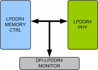
LPDDR4 DFI Verification IP provides an smart way to verify the LPDDR4 DFI component of a SOC or a ASIC.
LPDDR4 DFI Verification IP provides an smart way to verify the LPDDR4 DFI component of a SOC or a ASIC. The SmartDV's LPDDR4 DFI Verification IP is fully compliant with standard DFI Specification and provides the following features.
LPDDR4 DFI Verification IP is supported natively in SystemVerilog, VMM, RVM, AVM, OVM, UVM, Verilog, SystemC, VERA, Specman E and non-standard verification env
LPDDR4 DFI Verification IP comes with optional Smart Visual Protocol Debugger (Smart ViPDebug), which is GUI based debugger to speed up debugging.
Note: some files may require an NDA depending on provider policy.

LPDDR4 DFI Verification IP is a Protocol Bridge IP core from SmartDV Technologies listed on Semi IP Hub.
Engineers should review the overview, key features, supported foundries and nodes, maturity, deliverables, and provider information before shortlisting this Protocol Bridge IP.
Yes. Buyers can compare this product with similar semiconductor IP cores or IP families based on category, provider, process options, and structured technical specifications.