Overview
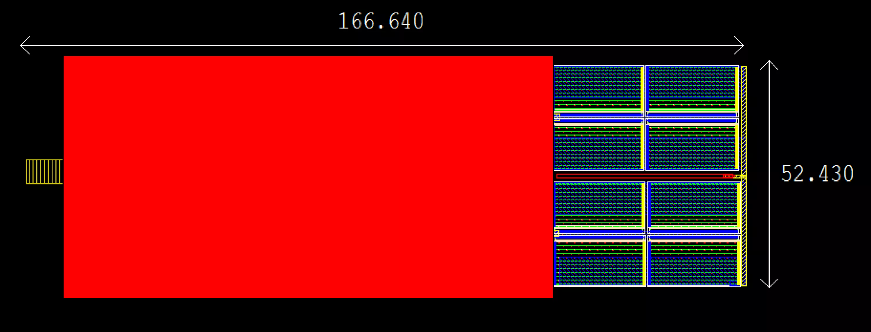
The CC-100IP-PI on Chip IP Block is an on-chip adjustable Impedance Controlled Hyper- capacitor with a Capacitance Multiplication, Series Inductance Nullification, Cybersecurity Enhancement and an Energy Harvesting capabilities. The impedance controlled Hyper-Bypass Capacitor IP creates an adjustable Impedance controlled point in IC power grids aiding in maximum on chip supply line filtering, Impedance matching for Power Grid flat frequency response, showing an up to a 600X improvement in effective and reservoir capacitance. The IP features a circuit noise activated dynamic input current controlled reservoir capacitance, and can function as a “stand-alone” on Chip DCAP, or work in parallel with existing DCAP structures. Due to the embedded IP negative feedback, the CC-100 features a 25% reduction in Hyper-Capacitor effective series inductance (ESL). The IP operates by feeding back a portion (nominally 20%) of the bypass current flowing through IP input base capacitors, feeding back current onto the chip power grid, preventing bypass Capacitor Deep discharge, thus reducing overall chip dynamic power draw. These effects substantially reduce RF Emissions from chip power grids making systems less vulnerable to cyber hacking and more secure. The IP draws no current for operation, thus maximizing block efficiency.
The Impedance Controlled Hyper Cap IP is meant to replace or work in parallel with existing on chip decoupling capacitors, thus can be shaped into various aspect ratios and sizes to fit on-chip “white space”, the area under power grids, etc. in the same fashion as typical on-chip decoupling capacitors. In similar fashion to typical decoupling capacitors, the IP blocks can be connected in parallel to increase overall Power Grid Impedance Matching, RF emission reduction, reservoir capability, and effective capacitance.
Learn more about Voltage Reference IP core
This white paper will discuss the design challenges that IC designers are facing when developing the new GDDR 7 high-performance memory interface and highlight some of the possible solutions to overcome these challenges, ensuring compliance and robustness of the GDDR7 memory interface.
The design of modern Application Specific Integrated Circuits (ASICs) and Systems on a Chip (SoCs) in advanced process nodes can be differentiated by the on-die integration of analog functions, such as power management. Vidatronic offers this white paper to give some historical background on this trend and delve specifically into the integration of power management. Vidatronic IP solutions and the benefits they bring to ASIC and SoC designers are discussed.
Based on the system specification of a typical smart meter, this article demonstrates the importance of carefully selecting the power metering IP solution so that its specification matches the standard requirements and copes with the application challenges. This article then pinpoints thoroughly the various issues that must be taken into account for the selection of the Silicon IP and helps identify the possible trade-offs between the performance of the Mixed-signal Front-end (MFE) and that of the Power and energy Computation Engine (PCE).
System integrators often encounter problems on application boards too late in the design cycle, when bringing together Virtual Components (ViCs of silicon IPs) into a system. Some ViC performances may be degraded at higher levels (SoC and PCB), and thus the final system does not perform as well as expected. In other words, assembling high-performance ViCs together does not guarantee high-performance SoCs or systems when fundamental integration aspects are not addressed or key issues are violated during the integration process.
Today’s energy metering standards demand higher accuracy and lower power consumption which, in turn, challenges system designers to deliver more competitive AFEs. This article reviews those challenges and presents a solution based on a multiplexed channel architecture that delivers ultra-high resolution, along with very low-power consumption and silicon area.
Presented in this paper is a tool that automatically migrates analog designs from one process to another while keeping circuit and layout topologies.