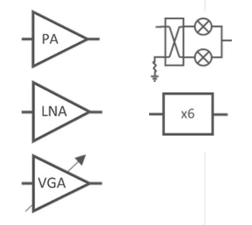
Overview
Our 28 nm Bulk CMOS IP portfolio comprises a wide selection of V- & E-band mmWave components, featuring best-in-class performance, small footprints, modular architectures and low�power consumption. The provided IP is Silicon-proven in TSMC's 28 nm HPC+RF CMOS process - but can be adapted to other foundries/nodes upon request. All mmWave & IF inputs/outputs are driven in differential-mode, optimized for an odd-mode characteristic impedance of 75 ? and 100 ?, respectively. A single VDD supply voltage of 0.9 V is used throughout, simplifying DC supply requirements & improving efficiency.
Each component’s layout is fully parameterized (PCell-based) and code-generated (incl. density fill and DRC compliance). There are no "hand-drawn" features. This allows for easier scalability, rapid integration, layout fine-tuning and detailed EM/linear/non-linear/stability design verification. All IP blocks are compatible with OA EDA tools, incl. Keysight ADS, Synopsys & Cadence. In addition, a full Keysight ADS workspace incl. all relevant testbenches and models is available for each component.
Physical bare-dies are available upon request
Learn more about RF Front End IP core
RF front-ends for GSM mobile handsets continue down path of integration
Micros benefit from ASIC heritage
Tools for Test and Debug : Specialized net backplanes needed for DSP debug in distributed environments
Software radio closes in on handsets
DSP/ASIC approach offers processing benefits for 802.11b implementation
Like most types of circuits, there is no such thing as a "one size fits all" PLL. This article will explore the trade-offs in PLL performance and design and look for a solution to most SOC PLL needs.