How Secure DDR Interfaces Protect DRAM from Memory Attacks
Brett Murdock, Dana Neustadter (Synopsys)
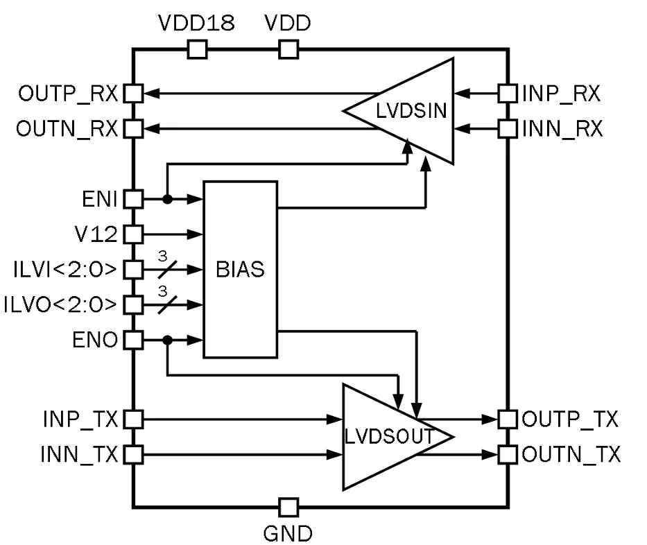
090TSMC_LVDS_02 consists of transmitter (LVDSOUT), receiver (LVDSIN) and a bias.
090TSMC_LVDS_02 consists of transmitter (LVDSOUT), receiver (LVDSIN) and a bias. The LVDS transmitter consists of a current source (nominal 3.5mA) that drives the differential pair lines and common-mode regulator, which provides the output common-mode voltage signal equal 1.25V. The output current adjustment is defined by the digital code register ILVO<2:0>. The receiver has high DC input impedance, so the majority of driver current flows across the 100Ohm external termination resistor generating about 350mV across the receiver inputs. When the driver switches, it changes the direction of current flow across the resistor, thereby creating a valid logic state of “1” or “0”. That is, it transforms 35mV input signal to CMOS 1.8V output signal. The internal current setting is defined by digital code register ILVI<2:0>.
| Foundry | Node | Process | Maturity |
|---|---|---|---|
| TSMC | 90nm | CIS | Silicon Proven |
Note: some files may require an NDA depending on provider policy.

1.6 Gbps DDR Programmable LVDS Transmitter/Receiver is a DDR IP core from NTLab listed on Semi IP Hub. It is listed with support for tsmc Silicon Proven.
Engineers should review the overview, key features, supported foundries and nodes, maturity, deliverables, and provider information before shortlisting this DDR IP.
Yes. Buyers can compare this product with similar semiconductor IP cores or IP families based on category, provider, process options, and structured technical specifications.