Overview
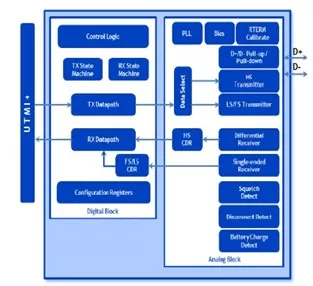
The entire physical layer (PHY) IP solution for USB 2.0 was created to provide exceptional performance and consume little power. The USB2.0 IP implements the High-Speed USB 2.0 Transceiver, which can be used with hosts, devices, or OTG function controllers. The specification that follows UTMI+level 3 is the USB2.0 PHY IP, which supports Full-Speed (12 Mbps) and Low-Speed (1.5 Mbps) data rates. By merging numerous mixed-signal circuits, high-speed data transfer @ 480Mbps can be accomplished. The expanded USB Battery Charging standards, intended for usage in consumer electronics and mobile devices, are also supported by the USB2.0 PHY IP. The USB 2.0 PHY IP standard is implemented by numerous factories and nodes, including "TSMC 28HPC+, TSMC 40LP, TSMC 40LL, UMC 28HPC, UMC 40LP, UMC 55SP, UMC 55EF, SMIC 14SF+, SMIC 40LL, SMIC 55LL." The USB2.0 PHY IP transceiver's small chip size and low power consumption had no impact on performance or data throughput. In order to fully allow host and device functionality, the USB2.0 PHY IP delivers a full on-chip physical transceiver solution with Electrostatic Discharge (ESD) protection, a clock generating block provided by an internal PLL, and a resistor termination calibration circuit.
Provider
T2M GmbH is the leading Global Technology Company supplying state of the art complex semiconductor connectivity IPs and KGDs, enabling the creation of complex connected devices for Mobile, IoT and Wearable markets.
T2M's unique SoC White Box IPs are the design database of mass production RF connectivity chips supporting standards including Wifi, BT, BLE, Zigbee, NFC, LTE, GSM, GNS. They are available in source code as well as KGD for SIP / modules.
With offices in USA, Europe, China, Taiwan, South Korea, Japan, Singapore and India, T2M’s highly experienced team provides local support, accelerating product development and Time 2 Market.
Learn more about Single-Protocol PHY IP core
UniversalFlash Storage (UFS) was created for mobile applications and computer systems requiring high performance and low power consumption. These systems typically use embedded Flash based on the JEDEC standard eMMC. UFS was defined by JEDEC as the evolutionary replacement for eMMC offering significantly higher memory bandwidth. The standard builds on existing standards such as the SCSI command set, the MIPI Alliance M-PHY and UniPro as well as eMMC form factors to simplify adoption and development.
In this paper, we introduce a new high-level, dataflow programming language called C~ (“C flow”) that further increases productivity by raising the level of abstraction from behavioral descriptions, while overcoming the limitations of C for hardware design. We present the syntax and semantics of this language, and the framework that provides hardware and software code generation. This paper illustrates the benefits of using C~ for hardware design of a IEEE 802.3 MAC, synthesized for FPGA and for 90nm CMOS technology.
Universal Flash Storage (UFS) was created for mobile applications and computer systems requiring high performance and low power consumption. These systems typically use embedded Flash based on the JEDEC standard eMMC. UFS was defined by JEDEC as the evolutionary replacement for eMMC offering significantly higher memory bandwidth. The standard builds on existing standards such as the SCSI command set, the MIPI Alliance M-PHY and UniProSM as well as eMMC form factors to simplify adoption and development.
Since MIPI and MDDI standards both target interfaces to cameras and displays on mobile devices, are two separate standards really needed?
Enter the Inner Sanctum of RapidIO: Part 1
Networking software key to PICMG 2.16 optimization