Overview
VESA introduced the first Display Stream Compression (DSC) standard in 2014. The DSC 1.1 has been incorporated into the VESA Embedded DisplayPort (eDP) and MIPI® DSI embedded mobile interface standards. The latest VESA Display Compression-M (VDC-M) standard has also been adopted into the MIPI DSI standard. For mobile applications, DSC 1.1 and VDC-M mainly serve to reduce the video interface data rate, which reduces system power, prolongs battery life, and reduces interconnects to enable sleeker designs. For external display interfaces, DSC 1.2b extends resolution across existing connectors and cables, enabling 8K video and legacy support from the same connection.
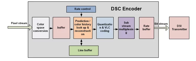
Being compliant with the VESA DSC 1.2a and 1.2b standards, the IP core supports various prediction schemes (MMAP, BP, MPP, ICH) as well as color formats in YCbCr and RGB. It transfers more pixel data over display links to save memory size in embedded frame buffers in display driver ICs and performs visually lossless compression, low gate count and latency for ultra-high-definition display applications. It can be easily integrated into ASIC and FPGA applications.
Features
- Compliant with the VESA DSC 1.2a and 1.2b standards
- Performs encoding
- Supports 8/10/12/14/16 bpc
- 4:4:4 RGB, 8, 10, and 12 bpc
- 4:4:4 YCbCr, 8, 10, and 12 bpc
- 4:2:2 YCbCr 8, 10, and 12 bpc
- 4:2:0 YCbCr, 8, 10, and 12 bpc
- Any mode, 14 and 16 bpc
- The encoder algorithm is optimized for hardware implementations at 1 pixel/clock (2 pixels/clock for Native 4:2:2 or 4:2:0 mode)
- Supports MMAP, BP, MPP and ICH
- High Performance Design
- 4K video at 60Hz
- 8K video at 30Hz (ASIC only)
Programmable display resolutions
Learn more about VESA DSC IP core
The integration of VESA Display Stream Compression (DSC) and MIPI Display Serial Interface (DSI) in a System-on-Chip (SoC) offers significant benefits for high-resolution display systems. This whitepaper discusses the challenges involved in integrating these technologies and provides insights into overcoming them.
From the first monochrome mobile displays to today’s ultra-high-definition automotive dashboards and immersive AR/VR headsets, MIPI technology has quietly become the backbone of modern data connectivity. Let’s explore how MIPI standards have evolved, the markets they serve, and why Rambus is at the forefront of this transformation.
Over the past decade, we have seen generations of new products with increasingly sophisticated display feature sets. Each new generation pushes the boundaries of display technology even further with higher resolutions, faster refresh rates, and increased pixel depth at the forefront of these developments.
As automotive displays become part of the safety surface, traditional host-dependent display architectures are showing their limits. In this article, Trilinear outlines how a RISC-V supervised DisplayPort subsystem can provide isolated control, deterministic fault handling, and a more auditable architecture for advanced automotive display platforms.