Provider
T2M GmbH is the leading Global Technology Company supplying state of the art complex semiconductor connectivity IPs and KGDs, enabling the creation of complex connected devices for Mobile, IoT and Wearable markets.
T2M's unique SoC White Box IPs are the design database of mass production RF connectivity chips supporting standards including Wifi, BT, BLE, Zigbee, NFC, LTE, GSM, GNS. They are available in source code as well as KGD for SIP / modules.
With offices in USA, Europe, China, Taiwan, South Korea, Japan, Singapore and India, T2M’s highly experienced team provides local support, accelerating product development and Time 2 Market.
Learn more about Single-Protocol PHY IP core
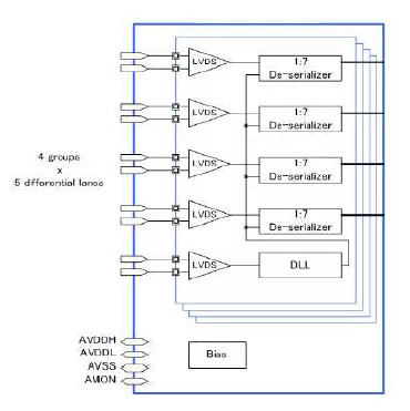
UniversalFlash Storage (UFS) was created for mobile applications and computer systems requiring high performance and low power consumption. These systems typically use embedded Flash based on the JEDEC standard eMMC. UFS was defined by JEDEC as the evolutionary replacement for eMMC offering significantly higher memory bandwidth. The standard builds on existing standards such as the SCSI command set, the MIPI Alliance M-PHY and UniPro as well as eMMC form factors to simplify adoption and development.
In this paper, we introduce a new high-level, dataflow programming language called C~ (“C flow”) that further increases productivity by raising the level of abstraction from behavioral descriptions, while overcoming the limitations of C for hardware design. We present the syntax and semantics of this language, and the framework that provides hardware and software code generation. This paper illustrates the benefits of using C~ for hardware design of a IEEE 802.3 MAC, synthesized for FPGA and for 90nm CMOS technology.
Universal Flash Storage (UFS) was created for mobile applications and computer systems requiring high performance and low power consumption. These systems typically use embedded Flash based on the JEDEC standard eMMC. UFS was defined by JEDEC as the evolutionary replacement for eMMC offering significantly higher memory bandwidth. The standard builds on existing standards such as the SCSI command set, the MIPI Alliance M-PHY and UniProSM as well as eMMC form factors to simplify adoption and development.
Since MIPI and MDDI standards both target interfaces to cameras and displays on mobile devices, are two separate standards really needed?
Enter the Inner Sanctum of RapidIO: Part 1
Networking software key to PICMG 2.16 optimization