9-bit 2-channel 0.5 to 33 MSPS (8 to 500 kHz BW) delta-sigma ADC
The block is second order delta-sigma ADC with 5-level quantizer.
Overview
The block is second order delta-sigma ADC with 5-level quantizer.
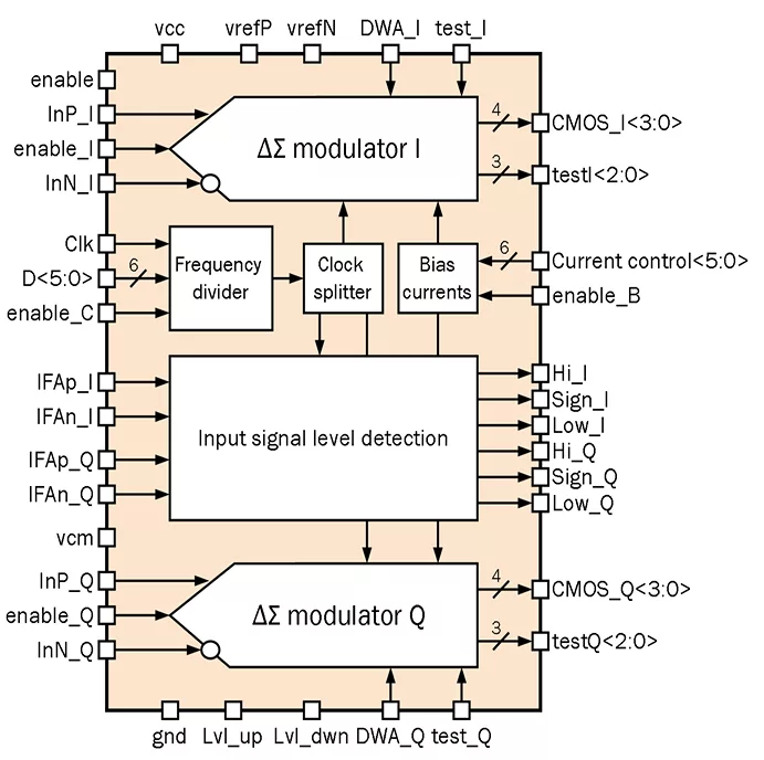
The block consists of:
- two integrating cascades based on switch capacitors technique;
- 5-level flash-ADC;
- tunable (6-bit control) clock signal frequency divider;
- clock splitter;
- block of bias currents, tunable (6-bit control);
- Data-Weighted Averaging (DWA) correction of capacitors mismatch;
- input signal level detection.
Output signal is represented in “thermometer” code. There is a possibility to disable of each channel, frequency divider, block of bias currents, DWA correction. There is an in-built output from frequency divider for clocking digital filters.
Input DC level is 0.9 V; recommended voltage levels for references are 0.9 ± 0.4 V; recommended input signal differential amplitude is 0.64 V; allowable deviation of clock duty cycle: 50 ± 5%.
The block is fabricated on iHP SiGe BiCMOS 0.25 um (SGB25V) technology.
Key features
- iHP SGB25V
- 2-channel wide-band delta-sigma ADC
- 9-bit resolution
- Information speed modes: 2.4 kBd – 512 kBd
- Supply voltage 1.8 V
- Tunable opamps current
- SFDR > 63 dB
- SNR > 60 dB
- Input differential signal range 1.6 V
- In-built input signal level detection, sign detection
- Portable to other technologies (upon request)
Block Diagram

Applications
- Analog to digital conversion of wide-band input signal
- Recievers, transmitters, transceivers
- Analog integral circuits
- Measuring equipment
- Medical equipment
What’s Included?
- Schematic or NetList
- Abstract model (.lef and .lib files)
- Layout view (optional)
- Behavioral model (Verilog)
- Extracted view (optional)
- GDSII
- DRC, LVS, antenna report
- Test bench with saved configurations (optional)
- Documentation
Specifications
Identity
Analog
Files
Note: some files may require an NDA depending on provider policy.
Provider

Learn more about ADC IP core
Time Interleaving of Analog to Digital Converters: Calibration Techniques, Limitations & what to look in Time Interleaved ADC IP prior to licensing
Three ways of looking at a sigma-delta ADC device
Specifying a PLL Part 1: Calculating PLL Clock Spur Requirements from ADC or DAC SFDR
Save power in IoT SoCs by leveraging ADC characteristics
High Speed ADC Data Transfer
Frequently asked questions about ADC IP cores
What is 9-bit 2-channel 0.5 to 33 MSPS (8 to 500 kHz BW) delta-sigma ADC?
9-bit 2-channel 0.5 to 33 MSPS (8 to 500 kHz BW) delta-sigma ADC is a ADC IP core from NTLab listed on Semi IP Hub.
How should engineers evaluate this ADC?
Engineers should review the overview, key features, supported foundries and nodes, maturity, deliverables, and provider information before shortlisting this ADC IP.
Can this semiconductor IP be compared with similar products?
Yes. Buyers can compare this product with similar semiconductor IP cores or IP families based on category, provider, process options, and structured technical specifications.