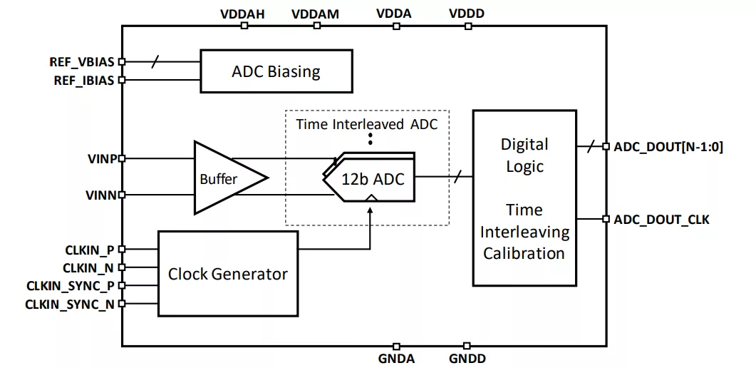
Overview
The ODT-ADS-12B5G-T28 is an ultra-highperformance time-interleaved ADC designed in a 28nm CMOS process.
This 12-bit, 5GSPS ADC supports input signals up to Nyquist and features a differential fullscale range of 0.8Vpp and excellent static and dynamic performance.
The ADC architecture is optimized to maximize performance while minimizing power and area consumption. The ADC input is internally buffered and then distributed to timeinterleaved ADC channels.
The ADC includes built in calibration to remove time interleaving artifacts, including offset mismatch, gain mismatch and timing skew.
To maximize SNR, the ADC includes an ultralow-jitter clock distribution network with aperture jitter of 50fsrms.
Provider

Omni Design Technologies, Inc.
HQ:
USA
Omni Design Technologies, Inc. is a developer of disruptive, ultra-low power semiconductor embedded circuits (IP Cores), including ultra-low power analog circuits, highly-efficient interface circuits and connected sensors. Our patented and proprietary technology offers solutions that use dramatically lower power and provide superior performance, architected from the ground up to take advantage of deep sub-micron CMOS processes. Omni Design’s mission is to provide a wide range of ultra low-power, high performance embedded circuits configured to enable highly-differentiated semiconductor systems and plug-and-play system-on-chip (SoC) development. Our IP offerings target SoCs that address a wide range of application areas including IoT, test and measurement, high speed interfaces, communications, medical imaging, and sensor hubs. Omni Design Technologies, Inc. is a privately held company with offices in Milpitas, CA and Boston, MA. Omni Design was founded in 2015 by a team of semiconductor industry veterans, technologists, and experienced entrepreneurs with a successful track record of delivering high performance analog solutions that advance the state of the art.
Learn more about ADC IP core
This paper introduces a novel closed-loop testing methodology for efficient linearity testing of high-resolution Successive Approximation Register (SAR) Analog-to-Digital Converters (ADCs). Existing test strategies, including histogram-based approaches, sine wave testing, and model-driven reconstruction, often rely on dense data acquisition followed by offline post-processing, which increases overall test time and complexity.
Analog to digital converters have three key input ports along with data output ports as per digital resolution requirements. These inputs ports are Analog Signal, Reference and Clock. If we compare across most of the converter architectures then clock frequency is directly related to output data rate and latency of the data conversion.
The growing availability of digital ICs like microcontrollers, microprocessors, and field-programmable gate arrays (FPGAs) allows developers to use complex digital processing techniques rather than analog signal conditioning. For this reason, analog-to-digital converters (ADCs) have become a widely-used component in mixed-signal circuits.
In high end RF systems, such as 5G radios, the requirements are so stringent that the source of this strongest unwanted tone can be the PLL. This article outlines how spurs in the input clock to the ADC or DAC may limit the SFDR. This in turn will set the requirements for the spurs for the input clock (from a PLL), in order to achieve a specific SFDR.
Power-sensitive applications such as Internet-of-Things (IoT) require a comprehensive power savings strategy within the system-on-chip (SoC). Techniques relying solely on the use of traditional power down modes and low supply voltage may not be enough to achieve the required power targets. The analog block is often assumed to be too sensitive and not compatible with aggressive power management techniques.
When continuously running a high speed ADC, it can be a challenge to deal with the firehose of raw data available at the output. To use City Semiconductor’s 2.5 GS/s 12-bit ADC, for example, 30 gigabits per second of data have to be accepted.