Vendor: Rambus, Inc. Category: PCI Express

PCIe 6.1 Controller

The PCI Express® (PCIe®) 6.1 Controller is configurable and scalable controller IP designed for ASIC implementation.

Overview

The PCI Express® (PCIe®) 6.1 Controller is configurable and scalable controller IP designed for ASIC implementation. The controller supports the PCIe 6.1 specification, including 64 GT/s data rates, PAM4 signaling, FLIT mode, and L0p power state. The PCIe 6.1 architecture will be essential for SoC designers creating next-generation chips that require the movement of large amounts of data within systems, including applications like HPC, cloud computing, artificial intelligence/machine learning (AI/ML), enterprise storage, networking, and automotive.

How the PCIe 6.1 Controller Works

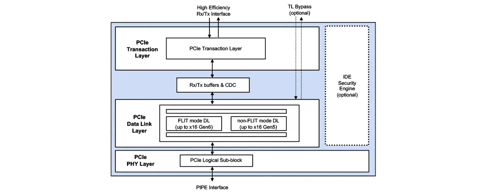
The PCIe 6.1 controller is backward compatible to the PCIe 5.0, 4.0 and 3.1/3.0 specifications. It supports version 6.x of the PHY Interface for PCI Express (PIPE) specification. The controller exposes a highly efficient transmit (Tx) and receive (Rx) interface with configurable bus widths. Designed to satisfy a multitude of customer and industry use cases, the IP can be configured to support endpoint, root port, switch port, and dual-mode topologies, allowing for a variety of use models. The provided Graphical User Interface (GUI) Wizard allows designers to tailor the IP to their exact requirements, by enabling, disabling, and adjusting a vast array of parameters.

The controller can be delivered standalone or integrated with the customer’s choice of PCIe 6 PIPE compliant SerDes. It can also be provided with example reference designs for integration with FPGA SerDes.

Key features

  • PCI Express layer
    • Designed to the latest PCI Express 6.1 (64 GT/s), 5.0 (32 GT/s), 4.0 (16 GT/s), 3.1/3.0 (8 GT/s), and PIPE 6.x (8, 16, 32, 64 and 128-bit) specifications
    • Supports SerDes Architecture PIPE 10b/20b/40b/80b width
    • Supports original PIPE 8b/16b/32b/64b/128b width
    • Compliant with PCI-SIG Single-Root I/O Virtualization (SR-IOV) Specification
    • Supports multiple virtual channels (VCs) in FLIT and non-FLIT modes
    • Supports Endpoint, Root-Port, Dual-mode, Switch port configurations
    • Supports PCIe 6.1 to PCIe 1.0 speeds
    • Supports Forward Error Correction (FEC) – Lightweight algorithm for low latency
    • Supports L0p Low Power mode
    • Up to 4-bit parity protection for data path
    • Supports Clock Gating and Power Gating
    • RAS features include LTSSM timers override, ACK/NAK/Replay/UpdateFC timers override, unscrambled PIPE interface access, error injection on Rx and Tx paths, recovery detailed status and much more, allowing for safe and reliable deployment of IP in mission-critical SoCs
  • User Interface layer
    • User-selectable Transaction/Application Layer clock frequency
    • Sideband signaling for PCIe configuration access, internal status monitoring, debug, and more
    • Optional Transaction Layer bypass
  • Integrity and Data Encryption (IDE) – Optional
    • Implements the PCI Express IDE ECN
    • Configurable IDE engine
    • Configurable data bus for PCIe IDE
    • Supports containment and skid modes
    • Supports multi-stream
    • Utilizes high-performance AES-GCM for encryption, decryption, authentication
    • PCIe IDE TLP aggregation for 1, 2, 4, 8 TLPs
    • PCIe IDE automatic IDE prefix insertion and detection
    • PCIe IDE automatic IDE sync/fail message generation
    • PCRC calculation & validation
    • Efficient key control/refresh
    • Bypass mode
  • Unique Features & Capabilities
    • Internal data path size automatically scales up or down based on max. link speed and width for reduced gate count and optimal throughput
    • Dynamically adjustable application layer frequency down to 8 Mhz for increased power savings
    • Optional MSI/MSI-X register remapping to memory for reduced gate count when SR-IOV is implemented
    • Configurable pipelining enables full speed operation on Intel and Xilinx FPGA, full support for production FPGA designs (when supported)
    • Ultra-low Transmit and Receive latency (excl. PHY)
    • Smart buffer management on receive side (Rx Stream) allows implementation of custom credit management schemes in the application logic
    • Merged Replay and Transmit buffer enables lower memory footprint
    • Advanced Reliability, Availability, Serviceability (RAS) features include LTSSM timers override, ACK/NAK/Replay/UpdateFC timers override, unscrambled PIPE interface access, error injection on Rx and Tx paths, recovery detailed status and much more, allowing for safe and reliable deployment of IP in mission-critical SoCs
    • Optional Transaction Layer bypass allows for customer specific transaction layer and application layer
    • Optional QuickBoot mode allows for up to 4x faster link training, cutting system-level simulation time by 20%

Block Diagram

Benefits

  • Optimized for high-bandwidth efficiency at data rates up to 64 GT/s
  • Scalable data path
  • Advanced PIPE modes and port bifurcation
  • Supports multiple virtual channels (VCs) in FLIT and non-FLIT modes
  • Supports Endpoint, Root-Port, Dual-mode, Switch port configurations
  • Advanced RAS features
  • Optional IDE security with AES-GCM encryption, decryption and authentication

Applications

  • Data Center
  • Edge
  • AI/ML
  • HPC

What’s Included?

  • IP files
    • Verilog RTL source code
    • Libraries for functional simulation
    • Configuration assistant GUI
  • Full Documentation
  • Reference Designs
    • Synthesizable Verilog RTL source code
    • Simulation environment and test scripts
    • Synthesis project & DC constraint files (ASIC)

Files

Note: some files may require an NDA depending on provider policy.

Specifications

Identity

Part Number
PCIe 6.1 Controller
Vendor
Rambus, Inc.

Provider

Rambus, Inc.
HQ: USA
Rambus delivers industry-leading chips and silicon IP for the data center and AI infrastructure. With over three decades of advanced semiconductor experience, our products and technologies address the critical bottlenecks between memory and processing to accelerate data-intensive workloads. By enabling greater bandwidth, efficiency and security across next-generation computing platforms, we make data faster and safer.

Learn more about PCI Express IP core

Challenges in PCI Express IP Implementation

IP selection, verification and integration are key aspects to the success of an IP-based design. This paper describes some of the challenges imposed by an IP based implementation of the technology and discusses about possible solutions to address them.

Realizing the Performance Potential of a PCI-Express IP

This paper describes challenges involved in realizing the maximum performance of a configurable interconnect IP (GPEX - Rambus PCI Express Digital Controller). The following sections describe how various performance metrics such as roundtrip latency and bandwidth can be used to characterize a PCI Express IP performance and its impact on the system. The ideas presented can also be applied to other high speed interconnect architectures like RapidIO and Hypertransport

Frequently asked questions about PCIe IP cores

What is PCIe 6.1 Controller?

PCIe 6.1 Controller is a PCI Express IP core from Rambus, Inc. listed on Semi IP Hub.

How should engineers evaluate this PCI Express?

Engineers should review the overview, key features, supported foundries and nodes, maturity, deliverables, and provider information before shortlisting this PCI Express IP.

Can this semiconductor IP be compared with similar products?

Yes. Buyers can compare this product with similar semiconductor IP cores or IP families based on category, provider, process options, and structured technical specifications.

×
Semiconductor IP