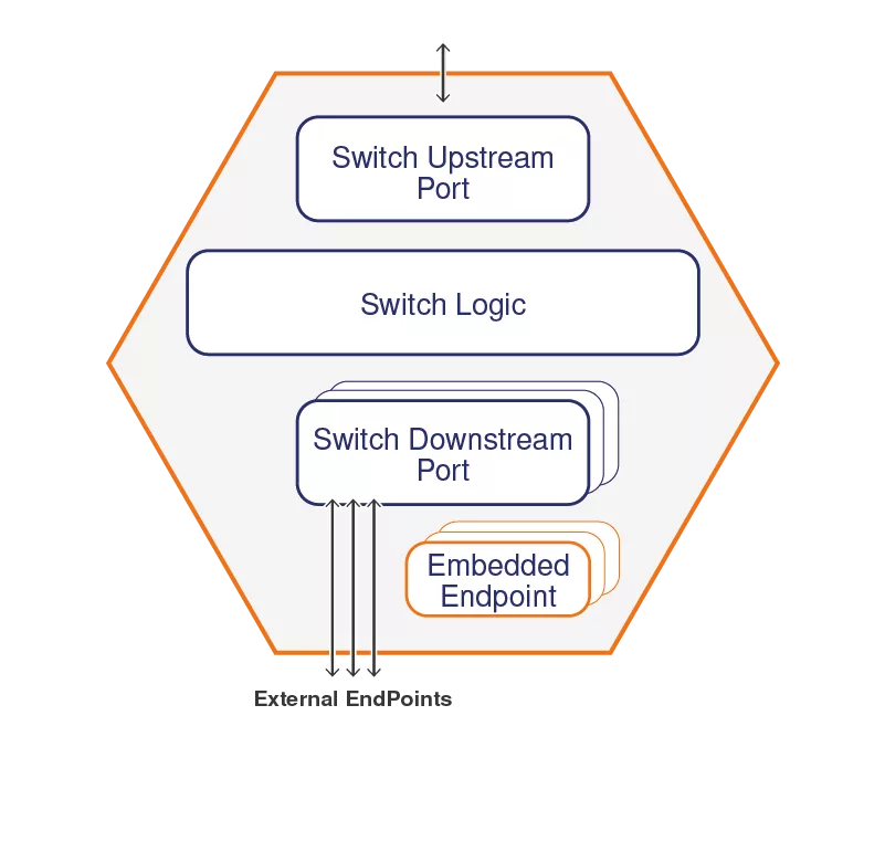
The PCIe 5.0 Multi-port Switch (formerly XpressSWITCH) is a customizable, multiport embedded Switch for PCIe designed for ASIC and FPGA implementations enabling the connection of one upstream port and up to 31 downstream ports.
How the PCIe 5.0 Multi-Port Switch Works
The PCIe 5.0 Switch IP transparently manages upstream-downstream data flow as well as peer-to-peer transfers between downstream ports, delivering the flexibility, scalability and configurability required for connecting multiple devices, including NVMe SSDs. It enables designers to use fewer PHYs, saving latency, power consumption and costs.
The PCIe 5.0 Multi-Port Swtich has been extensively verified using commercial and internally developed VIP and test suites. It is PCI-SIG certified since 2016 and is often used as an interoperability host platform for PCIe compliance testing.