Low-power, 16-bit RISC CPU with cache
The eSi-1650 16-bit CPU with instruction cache is targeted specifically for low-power applications, where typically an 8-bit CPU …
Overview
The eSi-1650 16-bit CPU with instruction cache is targeted specifically for low-power applications, where typically an 8-bit CPU may have previously been used or where a 32-bit CPU is too big or power hungry. The instruction cache provides a high performance, area and power efficient solution when running from on-chip NVM or Flash.
The use of the cache allows higher CPU frequencies when in mature technologies as frequency is typically limited by the memory speed. Power is reduced as a small cache require less power to read than flash. A cache can be much smaller than a full shadow RAM.
Even though it is 16-bit, the gate count is equivalent to many 8-bit cores due to the simplicity of the RISC pipeline. With a wider datapath and 16 general purpose registers, application programs are able to execute in far fewer clock cycles. This can save a significant amount of power by either allowing the CPU to be clocked at a lower frequency or by being able to enter a power down state sooner.
The eSi-1650’s instruction set includes a variety of arithmetic instructions such as a full 32-bit multiply, multiply and accumulate and divide. There are also a number of optional application specific instructions and addressing modes. Bit manipulation instructions such as bitfield extract and insert, count leading zeros, population count, find first set and bit reverse can be included. Integer square root, absolute value, min/max, CRC and parity are also available. Wait-for-interrupt instructions allow fast entry to low power states, enabling clock and power gating.
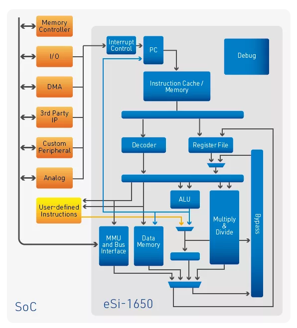
For those applications that require extreme performance or ultra low power operation, user-defined instructions and registers can be implemented.
The processor supports both user and supervisor operating modes, with privileged instructions and memory areas via the optional MPU, to allow an O/S kernel to be fully protected from user applications.
Hardware debug facilities include hardware breakpoints, watchpoints, trace, performance counters, null pointer detection and single-stepping for fast debugging of ROM, FLASH and RAM based programs.
Key features
- 16-bit RISC architecture
- 16 or 32 general purpose registers
- 92 basic instructions and 10 addressing modes
- Supports up to 74 user-defined instructions
- 5-stage pipeline
- Optional memory protection unit (MPU)
- Configurable instruction cache (1-64kB, direct mapped or 2 or 4 way associative)
- AMBA AHB buses and APB peripheral bus
- Optional support for user and supervisor modes
- Up to 16 vectored interrupts plus NMI and system call
- HW nested and prioritizable interrupts
- Fast interrupt response time of 6-9 cycles
- JTAG or serial debug, with optional trace and performance counters
- Up to 2.81 CoreMark per MHz
- Multiprocessor support
- Intermixed 16 and 32-bit instructions result in exceptional code density without compromising performance
- ASIC performance (Typical 28nm):
- Up to 1 GHz
- From 10k gates
- From 3.2uW/MHz
- High quality IP:
- Verilog RTL
- DFT ready
- Silicon proven
- C and C++ software development using license-free toolchain, under industry standard Eclipse IDE
- Easy migration path to a 16-bit version without caches or to a 32-bit version
Block Diagram

Specifications
Identity
Files
Note: some files may require an NDA depending on provider policy.
Provider

Learn more about CPU IP core
ChiPy®: Bridge Neural Networks and C++ on Silicon — Full Inference Pipelines with Zero CPU Round-Trips
Unleashing Leading On-Device AI Performance and Efficiency with New Arm C1 CPU Cluster
Encarsia: Evaluating CPU Fuzzers via Automatic Bug Injection
Introducing Cortex-A320: Ultra-efficient Armv9 CPU Optimized for IoT
Pie: Pooling CPU Memory for LLM Inference
Frequently asked questions about CPU IP cores
What is Low-power, 16-bit RISC CPU with cache?
Low-power, 16-bit RISC CPU with cache is a CPU IP core from eSi-RISC listed on Semi IP Hub.
How should engineers evaluate this CPU?
Engineers should review the overview, key features, supported foundries and nodes, maturity, deliverables, and provider information before shortlisting this CPU IP.
Can this semiconductor IP be compared with similar products?
Yes. Buyers can compare this product with similar semiconductor IP cores or IP families based on category, provider, process options, and structured technical specifications.