3.3 - 4.2V to -3.7V step-down DC/DC converter
180XFAB_DCDC_05 is capable to generate -4.2V ÷ -3.3V (-3.7V typical value) voltage and can maintain 50uA load for -3.7V output.
Overview
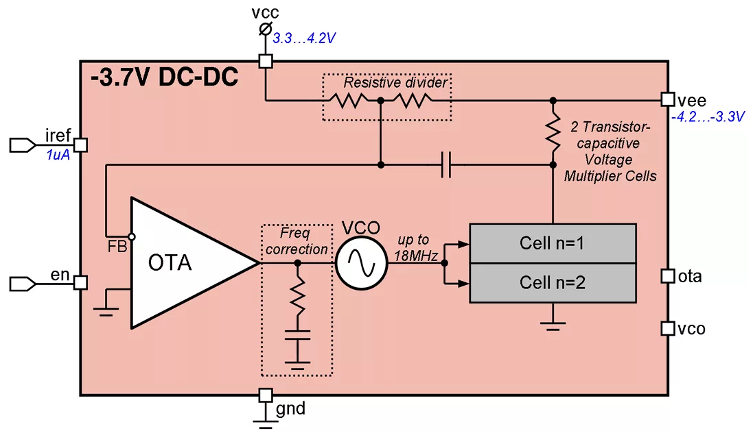
180XFAB_DCDC_05 is capable to generate -4.2V ÷ -3.3V (-3.7V typical value) voltage and can maintain 50uA load for -3.7V output. The block consists of OTA and transistor-capacitive multiplier cells. The DC/DC is used for forming negative supply. Upon power-up to typical 3.7V voltage at the fully charged 100nF output capacitor connected, slew rate of output voltage will be limited of the internal frequency correction circuits and is approximately 4.3 V/us. Start-up time is increased with increasing capacitor nominal value proportionally.
Key features
- XFAB XT018
- Input Voltage Range: 3.3V to 4.2V
- Output Voltage: minus input voltage
Block Diagram

Applications
- Low-Voltage, High-Density Systems
- Broadband, Networking, and Optical Communications Infrastructure
What’s Included?
- Schematic or NetList
- Abstract model (.lef and .lib files)
- Layout view (optional)
- Behavioral model (Verilog)
- Extracted view (optional)
- GDSII
- DRC, LVS, antenna report
- Test bench with saved configurations (optional)
- Documentation
Files
Note: some files may require an NDA depending on provider policy.
Specifications
Identity
Provider

Learn more about DC/DC Converter IP core
How to simplify switch-mode DC-DC converter design
Ruggedizing Buck Converters For Space And Other High Radiation Environments
Paving the way for the next generation audio codec for True Wireless Stereo (TWS) applications - PART 2 : Increasing play time
Breaking new energy efficiency records with advanced power management platform
Guide to Choosing the Best LDO for Your Application
Frequently asked questions about DC-DC Converter IP cores
What is 3.3 - 4.2V to -3.7V step-down DC/DC converter?
3.3 - 4.2V to -3.7V step-down DC/DC converter is a DC/DC Converter IP core from NTLab listed on Semi IP Hub.
How should engineers evaluate this DC/DC Converter?
Engineers should review the overview, key features, supported foundries and nodes, maturity, deliverables, and provider information before shortlisting this DC/DC Converter IP.
Can this semiconductor IP be compared with similar products?
Yes. Buyers can compare this product with similar semiconductor IP cores or IP families based on category, provider, process options, and structured technical specifications.