The CMS0033 ATSC 8-VSB Modulator with integrated Channel Coder has been designed specifically to implement the 8-VSB requirements of the ATSC Digital Television Standard (A/53).
The core provides all the necessary processing steps to modulate a single transport stream into a complex I/Q signal for input to a pair of DACs, or a DDS up-conversion DAC such as the AD9857(or AD9957). Optionally, the output can be selected as an IF to supply a signal DAC.
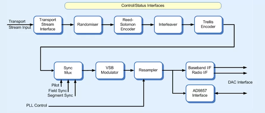
The design has been optimised to provide excellent performance in FPGA devices. A description of the processing steps follows:
Randomiser. This block performs energy dispersal by scrambling the incoming transport stream packets with a pseudo-random sequence.
Reed-Solomon Encoder. This block constructs 207-byte Reed Solomon codewords by applying a T=10 (207,187) code to the scrambled transport stream packets.
Interleaver. This block uses convolutional byte interleaving to disperse the Reed Solomon codewords over a period of approximately 4ms.
Convolutional Encoder. This block applies a rate 2/3 convolutional code to the interleaved data by means of a 4-state trellis encoder. The 3-bit encoder output symbols are mapped to 8-level 8 VSB constellation points.
Sync Multiplexer. This block inserts Field Sync and Segment Sync sequences into the transmitted symbol stream and adds a low-level Pilot signal. These signals are used for physical-layer synchronisation at the receiver.
VSB Modulation. This block performs vestigial sideband modulation of a locally-generated baseband carrier, driven by the composite output from the Sync Multiplexer.
Rate Conversion. This block re-samples the complex samples output from the VSB Modulation block at symbol-rate into complex samples at a sub multiple of the DAC/core clock frequency.
A frequency control input is provided to allow the modulation symbol rate to be locked to the data rate on the transport stream interface. This would typically be driven by a PLL, for example when the SMPTE 310M interface option is selected.
Baseband-to-IF. This block provides the option to mix the signal up to a higher IF as defined by a software register. The block may be removed using synthesis options if it is not required.
Radio Interface. This block performs some final, register-selectable processing functions to optimise the output for the radio in the target application. For example, the data can be formatted to work with either twos-complement or offset-binary DAC devices. In addition the data is formatted to suit the external device that could take separate I/Q, multiplexed I/Q or a single IF output.
Additional modes are provided to support the Analog Devices AD9857 device that provide up conversion, SINC filtering and DAC functions in a single package. The AD9857 device requires that the I/Q data be multiplexed onto a single data bus. The ad9857_pdclk input is provided to enable this feature and should be sourced from the AD9857 PDCLK output
Control/Status Interface. The Control/Status interface is provided by a synchronous, 32-bit register bank. Full details of the registers within the modulator core are contained within the full data sheet.