Vendor: Agile Analog Category: ADC

12-bit Analog-to-Digital Converter

The agileADC 12 Analog-to-Digital Converter is a traditional Charge-Redistribution SAR ADC that is referenced to VDD, VSS.

Overview

The agileADC 12 Analog-to-Digital Converter is a traditional Charge-Redistribution SAR ADC that is referenced to VDD, VSS. The architecture can achieve up to 12-bit resolution at sample rates up to 64 MSPS. It includes a 16-channel input multiplexor that can be configured to be buffered or unbuffered, and support differential or single-ended inputs.

Agile Analog designs are based on tried and tested architectures to ensure reliability and functionality. Our design methodology is programmatic, systematic and repeatable leading to analog IP that is more verifiable, more robust and more reliable. Our methodology also allows us to quickly re-target our IP to different process options. We support all the major foundries including TSMC, GlobalFoundries, Intel Foundry, Samsung Foundry, UMC and Other Foundries.

Key features

  • Resolution: 12 bits
  • Sampling Rate (Fs) 1: Up to 64 MSPS
  • Input Signal Bandwidth: Fs/2
  • SINAD1: Typ 69 dB
  • ENOB1: Typ 11.3 bits
  • SFDR1: Typ 90 dBc
  • INL: +/2 LSB
  • DNL: +/-1 LSB
  • Monotonic and no missing codes
  • Up to 16 input channels
  • Integrated reference generator
  • Integrated calibration mode

Block Diagram

Benefits

  • Digitally Wrapped
  • - AMBA-APB Interface to simplify integration, testing and operation.
  • - Provided with System Verilog models
  • DFT/DFM
  • - Incorporated trim and calibration to facilitate process and/or manufacturing offsets to be adjusted
  • - Built-in test mode
  • Configurable Inputs
  • - Up to 16 input channels
  • - Buffer or unbuffered
  • - Differential or Single-ended

Applications

  • IoT, Security, Automotive, AI, SoCs, ASICs

What’s Included?

  • Datasheet
  • Testing and Integration Guide
  • Verilog Models
  • Floorplan (LEF)
  • Timing models (LIB)
  • Netlist (CDL)
  • Layout (GDS)
  • Physical Verification Report
  • Design Report

Files

Note: some files may require an NDA depending on provider policy.

Specifications

Identity

Part Number
agileADC 12
Vendor
Agile Analog
Type
Silicon IP

Analog

Resolution bits
12 Bit

Provider

Agile Analog
HQ: United Kingdom
Agile Analog is transforming the world of analog IP with Composa™, its innovative, configurable, multi-process analog IP technology. Headquartered in Cambridge, UK, with a growing number of partners and customers across the globe, Agile Analog has developed a unique way to automatically generate analog IP that meet the customer’s exact specifications on almost any process from any foundry. The company provides a wide and ever expanding selection of analog IP and subsystems for power management, data conversion, IC health and monitoring, security and always-on domains. Agile Analog's novel approach utilises tried and tested analog circuits within its Composa library to create customised and verified analog IP solutions. This reduces the time to market and increases quality, helping to accelerate innovation in semiconductor design.

Learn more about ADC IP core

Uncertainty-Guided Live Measurement Sequencing for Fast SAR ADC Linearity Testing

This paper introduces a novel closed-loop testing methodology for efficient linearity testing of high-resolution Successive Approximation Register (SAR) Analog-to-Digital Converters (ADCs). Existing test strategies, including histogram-based approaches, sine wave testing, and model-driven reconstruction, often rely on dense data acquisition followed by offline post-processing, which increases overall test time and complexity.
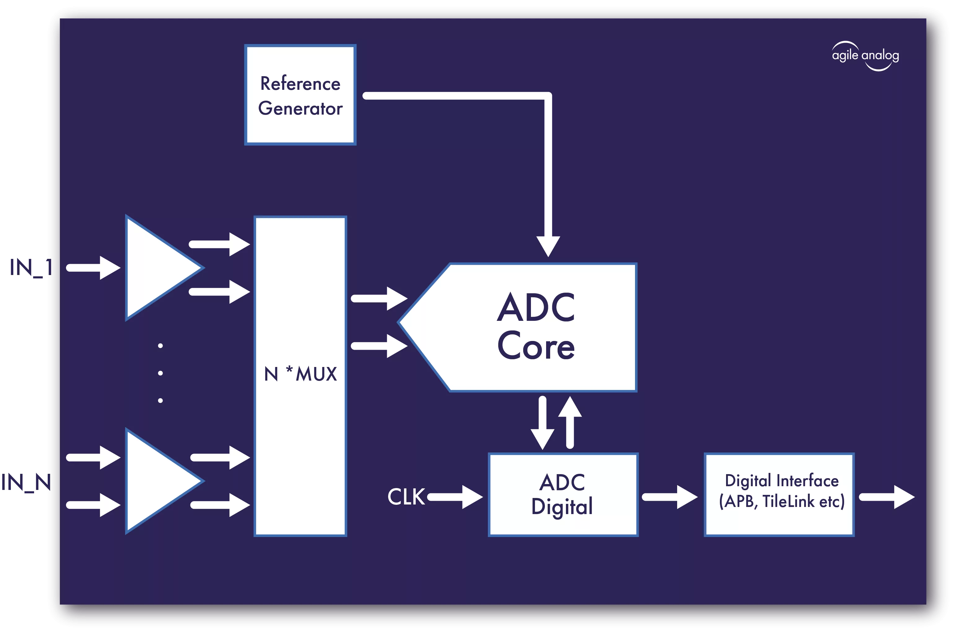
Three ways of looking at a sigma-delta ADC device

The growing availability of digital ICs like microcontrollers, microprocessors, and field-programmable gate arrays (FPGAs) allows developers to use complex digital processing techniques rather than analog signal conditioning. For this reason, analog-to-digital converters (ADCs) have become a widely-used component in mixed-signal circuits.

Specifying a PLL Part 1: Calculating PLL Clock Spur Requirements from ADC or DAC SFDR

In high end RF systems, such as 5G radios, the requirements are so stringent that the source of this strongest unwanted tone can be the PLL. This article outlines how spurs in the input clock to the ADC or DAC may limit the SFDR. This in turn will set the requirements for the spurs for the input clock (from a PLL), in order to achieve a specific SFDR.

Save power in IoT SoCs by leveraging ADC characteristics

Power-sensitive applications such as Internet-of-Things (IoT) require a comprehensive power savings strategy within the system-on-chip (SoC). Techniques relying solely on the use of traditional power down modes and low supply voltage may not be enough to achieve the required power targets. The analog block is often assumed to be too sensitive and not compatible with aggressive power management techniques.

High Speed ADC Data Transfer

When continuously running a high speed ADC, it can be a challenge to deal with the firehose of raw data available at the output. To use City Semiconductor’s 2.5 GS/s 12-bit ADC, for example, 30 gigabits per second of data have to be accepted.

Frequently asked questions about ADC IP cores

What is 12-bit Analog-to-Digital Converter?

12-bit Analog-to-Digital Converter is a ADC IP core from Agile Analog listed on Semi IP Hub.

How should engineers evaluate this ADC?

Engineers should review the overview, key features, supported foundries and nodes, maturity, deliverables, and provider information before shortlisting this ADC IP.

Can this semiconductor IP be compared with similar products?

Yes. Buyers can compare this product with similar semiconductor IP cores or IP families based on category, provider, process options, and structured technical specifications.

×
Semiconductor IP